Nano & Microfabrication
Manufacturing Mastery
Manufacturing Systems & Process Foundations
Process taxonomy, physics, DFM/DFA, production economics, Theory of ConstraintsCasting, Forging & Metal Forming
Sand/investment/die casting, open/closed-die forging, rolling, extrusion, deep drawingMachining & CNC Technology
Cutting mechanics, tool materials, GD&T, multi-axis machining, high-speed machining, CAMWelding, Joining & Assembly
Arc/MIG/TIG/laser/friction stir welding, brazing, adhesive bonding, weld metallurgyAdditive Manufacturing & Hybrid Processes
PBF, DED, binder jetting, topology optimization, in-situ monitoringQuality Control, Metrology & Inspection
SPC, control charts, CMM, NDT, surface metrology, reliabilityLean Manufacturing & Operational Excellence
5S, Kaizen, VSM, JIT, Kanban, Six Sigma, OEEManufacturing Automation & Robotics
Industrial robotics, PLC, sensors, cobots, vision systems, safetyIndustry 4.0 & Smart Factories
CPS, IIoT, digital twins, predictive maintenance, MES, cloud manufacturingManufacturing Economics & Strategy
Cost modeling, capital investment, facility layout, global supply chainsSustainability & Green Manufacturing
LCA, circular economy, energy efficiency, carbon footprint reductionAdvanced & Frontier Manufacturing
Nano-manufacturing, semiconductor fabrication, bio-manufacturing, autonomous systemsNano-manufacturing operates at scales from 1-100 nanometers — where quantum mechanics governs material behavior and a single atom matters. At this scale, materials exhibit extraordinary properties: gold nanoparticles appear red (not gold), carbon nanotubes are 100× stronger than steel at 1/6th the weight, and quantum dots emit precise wavelengths of light. Manufacturing at this frontier requires entirely different paradigms from macro-scale production.
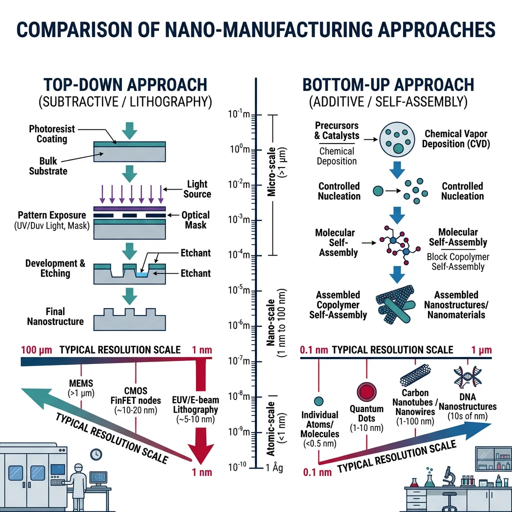
| Approach | Method | Resolution | Throughput | Application |
|---|---|---|---|---|
| Top-Down | EUV lithography (13.5 nm) | Sub-3 nm features | High (wafer-scale) | Semiconductor IC patterning |
| Focused Ion Beam (FIB) | ~5 nm | Very low (serial) | TEM sample prep, mask repair, prototyping | |
| Nanoimprint lithography (NIL) | Sub-10 nm | Medium (stamp-based) | Optical filters, anti-reflective coatings, bio-sensors | |
| Bottom-Up | Chemical Vapor Deposition (CVD) | Atomic layer | Medium (batch) | Graphene, CNT, thin films |
| Molecular self-assembly | ~1 nm | Inherently parallel | Block copolymer patterning, drug delivery capsules | |
| DNA origami | ~6 nm | Low (lab-scale) | Nanoscale templates, drug carriers (research stage) |
MEMS & NEMS Fabrication
MEMS (Micro-Electro-Mechanical Systems) integrate mechanical elements (beams, diaphragms, gears) with electronics on a single silicon chip at the micrometer scale. They are found in every smartphone (accelerometer, gyroscope, microphone, pressure sensor) and every modern car (airbag sensor, tire pressure monitor). The global MEMS market exceeds $15 billion annually.
Case Study: Bosch MEMS — The Invisible Revolution
Bosch is the world's largest MEMS manufacturer, producing 4+ billion sensors per year at its Reutlingen fab:
- Deep Reactive Ion Etching (DRIE): Bosch's patented process alternates etching (SF₆) and passivation (C₄F₈) cycles to create vertical trenches with >50:1 aspect ratios — the foundation of all their accelerometers and gyroscopes
- 1000× cost reduction: The BMI160 6-axis IMU (accelerometer + gyroscope) costs approximately $0.50 in volume — a device that would have cost $50,000 in 1990s laboratory equipment
- Wafer-level packaging: MEMS dies are encapsulated at wafer level using anodic bonding (glass-silicon) or fusion bonding (silicon-silicon), creating hermetic cavities at near-zero per-device cost
- Testing challenge: Each MEMS sensor has mechanical resonant behavior that must be characterized — Bosch tests every die on the wafer using automated probe stations with vibrational stimulus
Thin Film Deposition & Patterning
Thin film deposition — applying layers from sub-nanometer to several micrometers — is the foundational technique of nano-manufacturing. Every semiconductor chip, solar cell, display, and optical coating relies on precise thin film processes:
| Process | Mechanism | Thickness Control | Temperature | Key Applications |
|---|---|---|---|---|
| ALD (Atomic Layer Deposition) | Self-limiting surface reactions, one atomic layer per cycle | ±0.1 Å (sub-angstrom) | 100-400°C | High-k gate dielectrics (HfO₂), barrier layers, conformal coatings |
| CVD (Chemical Vapor Deposition) | Gas-phase precursors react on heated substrate | ±1-5% | 300-1000°C | SiO₂, Si₃N₄, polysilicon, graphene, diamond-like carbon |
| PVD (Sputtering) | Plasma ions eject target atoms onto substrate | ±2-5% | RT-300°C | Metal interconnects (Cu, Al), tool coatings (TiN, CrN) |
| Evaporation | Thermal or e-beam evaporation in vacuum | ±5-10% | RT (substrate) | Optical coatings, OLED organic layers, metallization |
| MBE (Molecular Beam Epitaxy) | Ultra-pure molecular beams in UHV | Single monolayer | 400-800°C | III-V compound semicon (GaAs, InP), quantum wells, HEMTs |
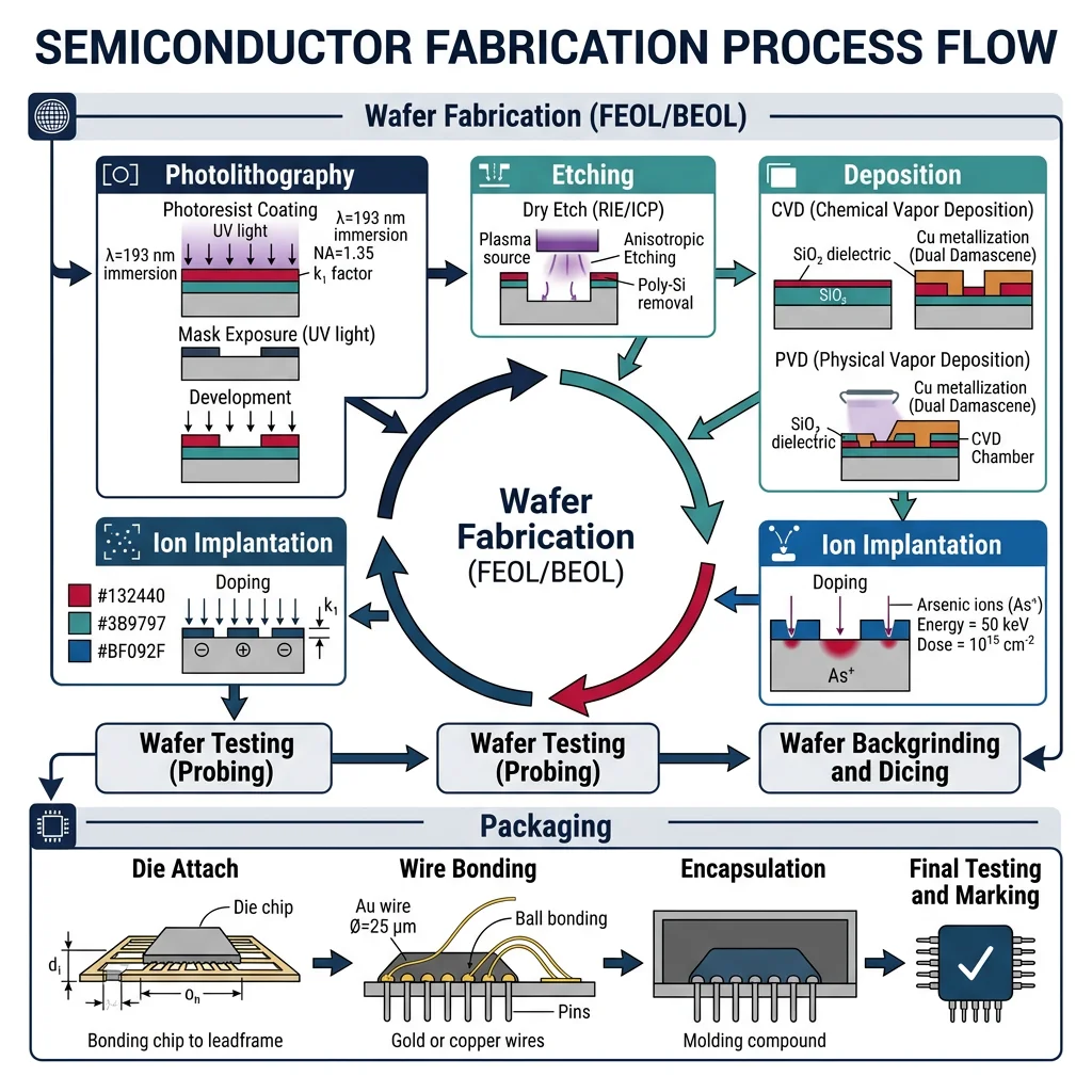
Semiconductor Manufacturing
Semiconductor fabrication is humanity's most precise and complex manufacturing process. A modern processor contains 100+ billion transistors patterned at 3 nm or below, using 1,000+ process steps over 3-4 months, in facilities costing $20-30 billion. The industry follows Moore's Law: transistor density doubles roughly every 2 years, driving relentless innovation.
import numpy as np

# Moore's Law — Transistor Density & Process Node Evolution
# Historical and projected semiconductor scaling

# Historical data: (year, process_node_nm, transistors_millions)
nodes = [
    (1971,  10000,   0.002),     # Intel 4004 — 10µm, 2,300 transistors
    (1978,  3000,    0.029),     # Intel 8086 — 3µm
    (1985,  1500,    0.275),     # Intel 386 — 1.5µm
    (1993,  600,     3.1),       # Pentium — 0.6µm
    (1999,  250,     9.5),       # Pentium III — 250nm
    (2004,  90,      125),       # Prescott — 90nm
    (2007,  65,      291),       # Core 2 — 65nm
    (2010,  32,      1160),      # Westmere — 32nm
    (2014,  14,      1750),      # Broadwell — 14nm
    (2017,  10,      8000),      # A11 Bionic — 10nm
    (2020,  5,       15000),     # A14 Bionic — 5nm (TSMC)
    (2022,  3,       25000),     # A17 Pro — 3nm (TSMC N3)
    (2025,  2,       50000),     # Expected — 2nm (TSMC N2, Samsung 2nm GAA)
]

years = [n[0] for n in nodes]
node_nm = [n[1] for n in nodes]
transistors = [n[2] for n in nodes]

print("Moore's Law — Semiconductor Scaling History")
print("=" * 65)
print(f"{'Year':<6} {'Node':<10} {'Transistors':<18} {'Density (MTr/mm²)'}")
print("-" * 65)

for yr, node, tr in nodes:
    # Approximate die area for density calculation
    if node >= 1000:
        density = tr / 100  # rough estimate
    else:
        density = tr / (100 * (node/14)**2)  # scaled to 14nm reference
    print(f"{yr:<6} {node:>6} nm   {tr:>12,.0f} M   {density:>10,.1f}")

# Scaling math
print(f"\nScaling overview (54 years):")
print(f"  Node shrink:       {nodes[0][1]/nodes[-1][1]:,.0f}× (10µm → 2nm)")
print(f"  Transistor growth:  {nodes[-1][2]/nodes[0][2]:,.0f}× (2,300 → 50B)")
print(f"  Doubling period:   ~{54*np.log(2)/np.log(nodes[-1][2]/nodes[0][2]):.1f} years (actual)")

# Cost of manufacturing
print(f"\nFab cost scaling:")
costs = [(2000, 1.5), (2005, 3), (2010, 5), (2015, 10), (2020, 18), (2024, 28)]
for year, cost in costs:
    print(f"  {year}: ${cost:.0f}B")
Cleanroom & Yield Management
Yield management — the percentage of functional dies per wafer — is the primary determinant of semiconductor profitability. At a 3 nm node with 1,000+ process steps, even 99.99% per-step yield results in only ~90% final die yield. A single process excursion can destroy $50,000+ worth of wafers.
| Yield Factor | Root Cause | Detection Method | Mitigation |
|---|---|---|---|
| Random defects | Particles, contamination, scratches | Optical/e-beam wafer inspection, defect review SEM | Cleanroom protocols, equipment PM, filter upgrades |
| Systematic defects | Lithography focus/dose, etch uniformity, CMP dishing | In-line metrology (OCD, SEM-CD), electrical test | APC (Advanced Process Control), recipe optimization |
| Parametric failures | Vth shift, leakage, resistance variation | WAT (Wafer Acceptance Test), e-test | Implant dose tuning, anneal optimization |
| Design-process interaction | Hotspot patterns, weak printability | DFM (Design for Manufacturability) checks, OPC verification | Design rule compliance, litho-friendly design |
Advanced Packaging & 3D IC
Advanced packaging has become the new frontier of performance scaling — as transistor shrinking slows and costs escalate, the industry is turning to "More than Moore" approaches: stacking chips vertically, integrating heterogeneous chiplets, and using advanced interconnects.
| Technology | Description | Interconnect Density | Example Products |
|---|---|---|---|
| 2.5D (Interposer) | Chiplets on silicon interposer with through-silicon vias (TSVs) | ~1000 bumps/mm² | AMD EPYC (TSMC CoWoS), NVIDIA H100 |
| 3D stacking (HBM) | Memory dies stacked vertically with microbumps + TSVs | ~2000 bumps/mm² | HBM3E (SK Hynix), DRAM stacks |
| Fan-Out Wafer Level (FOWLP) | Redistributed dies in molded wafer, no substrate | ~500 I/O/mm² | Apple A-series (TSMC InFO) |
| Chiplet + UCIe | Modular die-to-die with Universal Chiplet Interconnect | Standard: variable | Intel Ponte Vecchio, AMD MI300 |
| Hybrid Bonding | Direct Cu-Cu bonding at sub-1µm pitch, no bumps | >10,000/mm² | Sony image sensors, TSMC SoIC, AMD 3D V-Cache |
Bio-Manufacturing & Composites
Bio-manufacturing harnesses biological systems — cells, enzymes, organisms — as production platforms. Rather than mining, smelting, and machining, bio-manufacturing grows materials and chemicals using engineered microorganisms in bioreactors. This $500+ billion emerging sector promises to produce everything from spider silk to therapeutic proteins to biofuels.
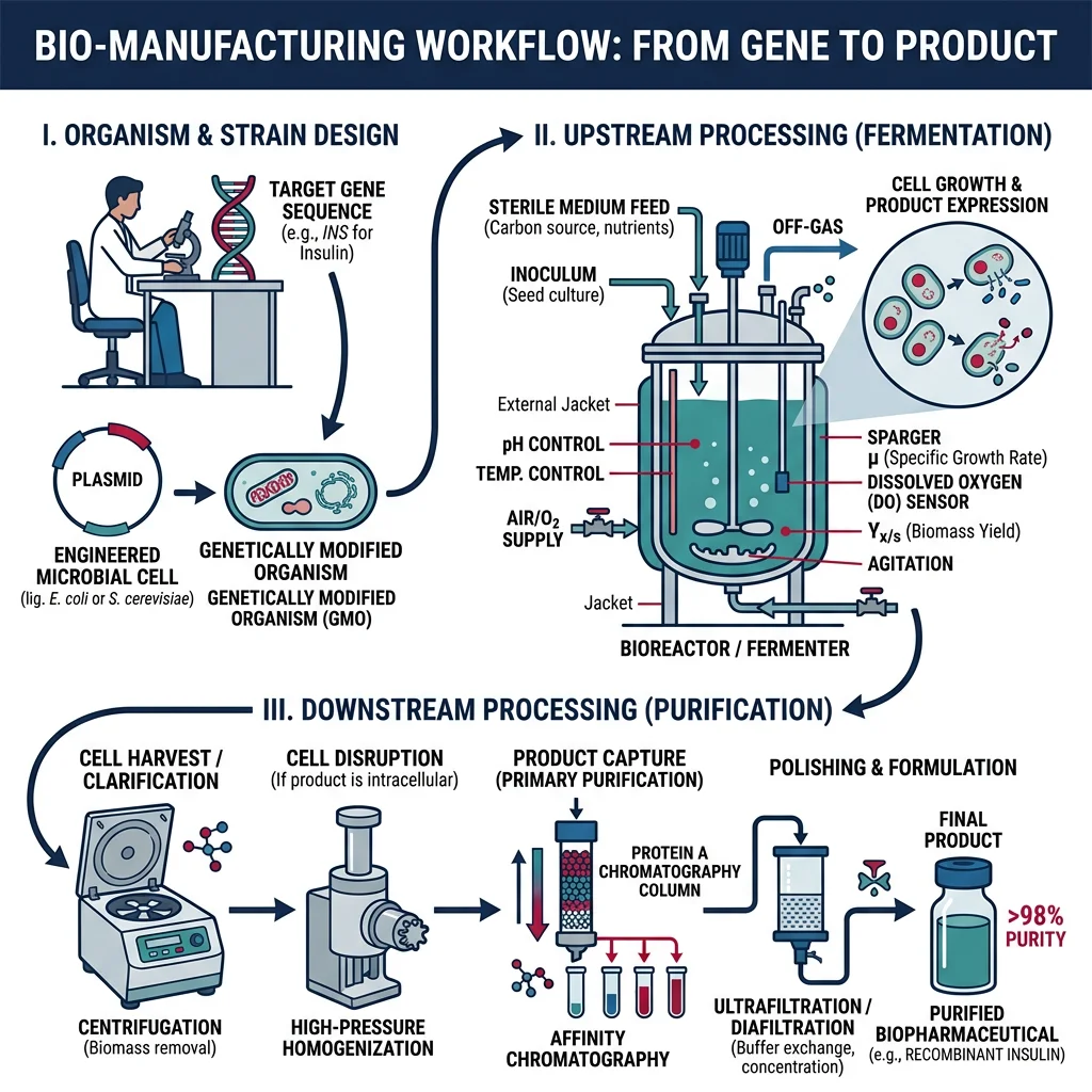
Case Study: Ginkgo Bioworks — The Organism Company
Ginkgo Bioworks operates the world's largest biological foundry — designing custom organisms that produce specific molecules at industrial scale:
- Platform model: Design-Build-Test-Learn cycle for engineering microorganisms — automated DNA assembly, high-throughput screening (100,000+ designs per program), and machine learning for pathway optimization
- Applications: Fragrances (engineered yeast produces high-value rose oil), food ingredients (fermentation-derived proteins), pharmaceuticals (biosynthetic cannabinoids), and agriculture (nitrogen-fixing microbes)
- Scale-up challenge: What works in a 1 mL lab well plate often fails at 10,000 L fermentation scale — mixing, oxygen transfer, metabolic byproduct accumulation change dramatically
- Cost trajectory: DNA synthesis cost has dropped 1,000× in 20 years (from $10/base to ~$0.01/base), enabling rapid prototyping of organism designs
Advanced Composites Automation
Advanced composites (CFRP, GFRP, ceramic matrix composites) offer exceptional strength-to-weight ratios but have historically been expensive and slow to manufacture. Automation is transforming composite production from craft to mass production:
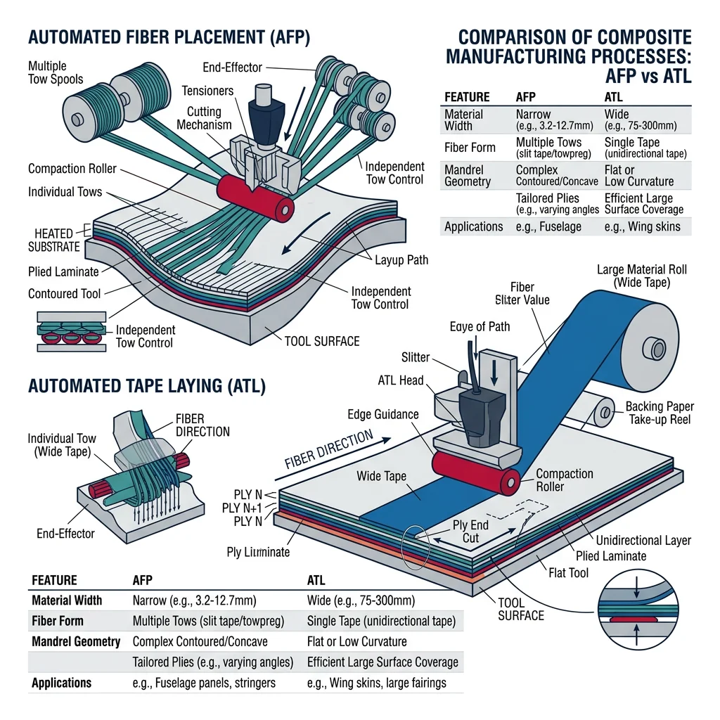
| Technology | Process | Rate | Part Type |
|---|---|---|---|
| AFP (Automated Fiber Placement) | Robot lays 8-32 tows of prepreg tape on complex contours | 10-25 kg/hr | Aircraft fuselage (Boeing 787), rocket fairings |
| ATL (Automated Tape Laying) | Wide tape (150-300mm) on flat or gentle curvature | 25-50 kg/hr | Wing skins, flat panels |
| RTM (Resin Transfer Molding) | Dry fiber preform + injected resin + heat cure | Minutes per part | Automotive structures (BMW i3 CFRP tub) |
| Thermoplastic composites | Stamp-forming, welding (ultrasonic/induction), in-situ consolidation | Seconds per part | Aircraft brackets, drone frames, sporting goods |
4D Printing & Smart Materials
4D printing adds the dimension of time to 3D printing — creating objects that change shape, properties, or function in response to external stimuli (heat, moisture, light, pH, magnetic field). The printed structure is programmed to transform after fabrication, enabling self-assembling structures and adaptive components.
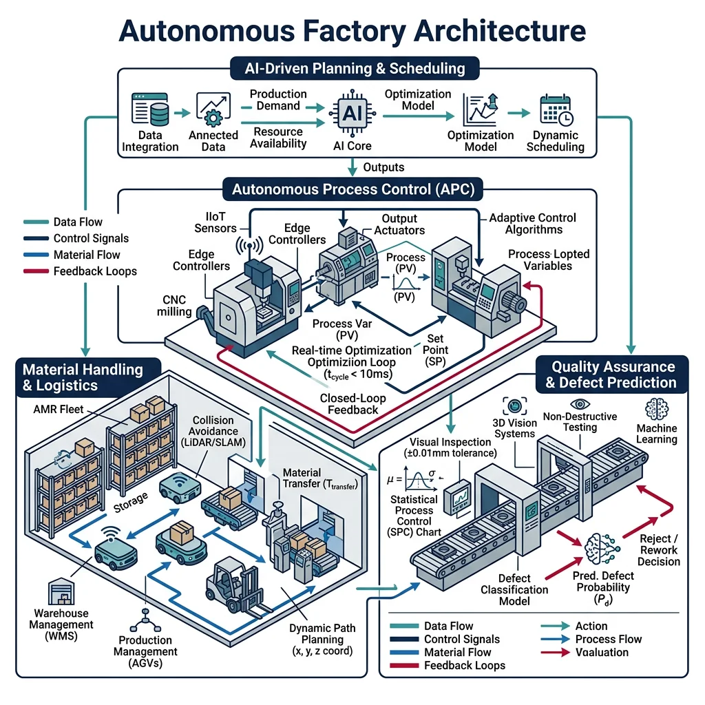
Autonomous & Future Systems
Autonomous manufacturing represents the ultimate convergence of AI, robotics, digital twins, and advanced materials — factories that design, optimize, produce, and quality-inspect products with minimal human intervention. This is not science fiction: elements are already operational at companies like FANUC (lights-out robot manufacturing), TSMC (AI-driven process control), and Relativity Space (AI-designed, 3D-printed rockets).
Case Study: Relativity Space — AI-Designed, 3D-Printed Rockets
Relativity Space's Terran R rocket represents the most radical rethinking of manufacturing in aerospace:
- Part count reduction: From ~100,000 parts (traditional rocket) to ~1,000 parts — 100× fewer through large-format metal 3D printing (Stargate: world's largest metal 3D printer)
- AI-driven design iteration: Each rocket iteration uses generative design + simulation to optimize structures — design-to-flight in 60 days (vs 2-4 years traditional)
- Factory footprint: Entire rocket produced in 1/10th the factory space of conventional aerospace manufacturing
- Material efficiency: Wire-arc DED process with titanium and aluminum alloys, buy-to-fly ratio approaching 1.2:1 (vs 10-20:1 in traditional aerospace machining)
import numpy as np

# Autonomous Manufacturing Maturity Assessment
# Framework for evaluating factory autonomy level

autonomy_dimensions = {
    "Planning & Scheduling": {
        "Level 1": "Manual scheduling by planners",
        "Level 2": "ERP-assisted scheduling with manual overrides",
        "Level 3": "AI-optimized scheduling with human approval",
        "Level 4": "Fully autonomous scheduling with exception alerts",
        "Level 5": "Self-learning scheduling that adapts to demand/disruptions"
    },
    "Process Control": {
        "Level 1": "Manual setups, operator-dependent parameters",
        "Level 2": "CNC programs, PLC-controlled sequences",
        "Level 3": "SPC with automatic parameter adjustment",
        "Level 4": "ML-based adaptive control, real-time optimization",
        "Level 5": "Self-tuning processes, autonomous recipe discovery"
    },
    "Quality Assurance": {
        "Level 1": "Post-process manual inspection",
        "Level 2": "Statistical sampling with gauges",
        "Level 3": "In-line automated inspection (vision, CMM)",
        "Level 4": "Predictive quality — AI flags defects before they occur",
        "Level 5": "Zero-defect manufacturing, self-correcting processes"
    },
    "Material Handling": {
        "Level 1": "Forklift and manual transport",
        "Level 2": "Conveyor systems, fixed automation",
        "Level 3": "AGVs with fixed routes",
        "Level 4": "AMRs with dynamic routing, automated warehousing",
        "Level 5": "Swarm robotics, self-organizing material flow"
    },
    "Maintenance": {
        "Level 1": "Reactive — fix when it breaks",
        "Level 2": "Preventive — scheduled intervals",
        "Level 3": "Condition-based — sensor monitoring",
        "Level 4": "Predictive — ML failure forecasting",
        "Level 5": "Self-healing — autonomous repair and part ordering"
    }
}

# Example assessment for a hypothetical factory
factory_scores = {
    "Planning & Scheduling": 3,
    "Process Control": 4,
    "Quality Assurance": 3,
    "Material Handling": 2,
    "Maintenance": 3,
}

print("Autonomous Manufacturing Maturity Assessment")
print("=" * 65)
print(f"\n{'Dimension':<25} {'Current':>8} {'Target':>8} {'Gap':>6}")
print("-" * 50)

total_current = 0
target = 4  # Industry 4.0 target level

for dim, score in factory_scores.items():
    gap = target - score
    total_current += score
    gap_display = f"+{gap}" if gap > 0 else "✓"
    print(f"{dim:<25} {'★' * score + '☆' * (5-score)}  {score}/5   {gap_display}")

avg_score = total_current / len(factory_scores)
print(f"\nOverall Maturity Score: {avg_score:.1f}/5.0")
print(f"Classification: {'Level ' + str(int(avg_score))} "
      f"({'Manual' if avg_score < 2 else 'Assisted' if avg_score < 3 else 'Semi-Autonomous' if avg_score < 4 else 'Largely Autonomous' if avg_score < 5 else 'Fully Autonomous'})")

print(f"\nPriority improvements:")
for dim, score in sorted(factory_scores.items(), key=lambda x: x[1]):
    if score < target:
        current_desc = autonomy_dimensions[dim][f"Level {score}"]
        next_desc = autonomy_dimensions[dim][f"Level {min(score+1, 5)}"]
        print(f"  {dim}: Level {score} → {score+1}")
        print(f"    FROM: {current_desc}")
        print(f"    TO:   {next_desc}")
Self-Configuring Production Lines
Self-configuring production lines dynamically reconfigure their physical layout, process parameters, and material flow in response to changing product requirements — eliminating the traditional trade-off between flexibility and efficiency.
Distributed Manufacturing Networks
Distributed manufacturing replaces centralized mega-factories with networks of smaller, geographically distributed production nodes — manufacturing products closer to the customer using digital designs transmitted over the internet. This model reduces logistics costs, enables mass customization, and builds supply chain resilience.
| Model | Description | Example | Key Technology |
|---|---|---|---|
| Cloud Manufacturing | On-demand access to shared manufacturing resources via platform | Xometry, Protolabs, Hubs (3D Hubs) | AI quoting, MES integration, digital twin |
| Micro-factories | Compact, modular factories deployable near demand | Arrival (EVs), Local Motors | Modular cells, robotic assembly, AM |
| Digital warehouse | Store designs not parts — print on demand near customer | Spare parts (Mercedes-Benz, Deutsche Bahn) | AM, digital inventory, blockchain traceability |
| Fab labs / makerspaces | Community-accessible manufacturing facilities | MIT Fab Lab network (2,500+ worldwide) | Desktop CNC, 3D printers, laser cutters |