Diffraction Techniques
Materials Science Mastery
Atomic Structure & Quantum Foundations
Quantum mechanics, bonding, band theory, Fermi energy, phononsCrystal Structures, Defects & Diffusion
FCC/BCC/HCP, Miller indices, dislocations, phase diagrams, Fick's lawsMetals & Alloys
Iron-carbon diagram, steels, aluminum, titanium, superalloys, heat treatmentPolymers & Soft Materials
Polymer chemistry, thermoplastics, viscoelasticity, rheology, biopolymersCeramics, Glass & Composites
Oxide ceramics, toughening, fiber-reinforced composites, interfacial bondingMechanical Behavior & Testing
Stress-strain, hardness, fatigue, fracture toughness, nanoindentationFailure Analysis & Reliability Engineering
Fractography, corrosion, tribology, root cause analysisNanomaterials & Smart Materials
Nanotubes, graphene, piezoelectrics, shape memory alloys, self-healingMaterials Characterization Techniques
XRD, SEM, TEM, AFM, DSC, TGA, spectroscopyThermodynamics & Kinetics of Materials
Gibbs free energy, CALPHAD, phase stability, solidificationElectronic, Magnetic & Optical Materials
Semiconductors, photovoltaics, dielectrics, superconductorsBiomaterials
Implants, biocompatibility, tissue engineering, drug deliveryEnergy Materials
Battery materials, hydrogen storage, fuel cells, nuclear materialsComputational Materials Science
DFT, molecular dynamics, FEM, materials informatics, AIX-Ray Diffraction (XRD)
X-ray diffraction is the most widely used technique for identifying crystalline phases and determining lattice parameters. When a beam of monochromatic X-rays strikes a crystalline sample, atoms in periodic planes scatter the radiation. Constructive interference occurs only when Bragg's Law is satisfied:
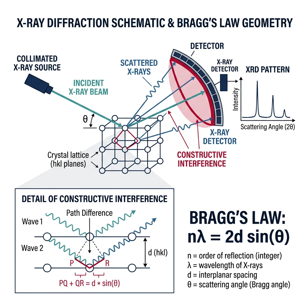
nλ = 2d sin θ
Where n is the diffraction order (an integer), λ is the X-ray wavelength (typically Cu Kα = 1.5406 Å), d is the interplanar spacing, and θ is the angle between the incoming beam and the crystal planes.
Key XRD Applications
- Phase Identification: Match diffraction peaks to known reference patterns — identify whether your steel contains austenite, ferrite, or martensite
- Lattice Parameter Determination: Precise peak positions yield unit cell dimensions (accuracy ~0.001 Å with careful calibration)
- Crystallite Size: Peak broadening reveals grain size via the Scherrer Equation: τ = Kλ / (β cos θ), where β is the full-width at half-maximum (FWHM)
- Residual Stress: Shifts in peak position at different specimen tilts quantify internal stresses (the sin²ψ method)
- Quantitative Phase Analysis: Rietveld refinement fits the entire diffraction pattern to determine weight fractions of multiple phases
Python Code: Bragg's Law Calculator
import numpy as np
import matplotlib.pyplot as plt

# Bragg's Law: n * lambda = 2 * d * sin(theta)
# Solving for d-spacing from measured 2-theta positions

wavelength = 1.5406  # Cu K-alpha in Angstroms

# Simulated 2-theta peak positions for BCC Iron (ferrite)
peak_2theta = np.array([44.67, 65.02, 82.33, 98.94, 116.38])  # degrees
hkl_labels = ['(110)', '(200)', '(211)', '(220)', '(310)']

# Calculate d-spacings
theta_rad = np.radians(peak_2theta / 2)  # Convert 2theta to theta in radians
d_spacings = wavelength / (2 * np.sin(theta_rad))

print("Bragg's Law: d-spacing Calculation for BCC Iron")
print("=" * 55)
print(f"{'Peak (hkl)':<12} {'2θ (°)':<10} {'θ (°)':<10} {'d (Å)':<10}")
print("-" * 55)
for i in range(len(peak_2theta)):
    print(f"{hkl_labels[i]:<12} {peak_2theta[i]:<10.2f} {peak_2theta[i]/2:<10.2f} {d_spacings[i]:<10.4f}")

# Calculate lattice parameter 'a' for each peak
# For BCC: d_hkl = a / sqrt(h^2 + k^2 + l^2)
hkl_values = [(1,1,0), (2,0,0), (2,1,1), (2,2,0), (3,1,0)]
a_values = []
for i, (h, k, l) in enumerate(hkl_values):
    a = d_spacings[i] * np.sqrt(h**2 + k**2 + l**2)
    a_values.append(a)

print(f"\nAverage lattice parameter a = {np.mean(a_values):.4f} Å")
print(f"Literature value for α-Fe:    a = 2.8665 Å")

# Plot simulated diffraction pattern
fig, ax = plt.subplots(figsize=(10, 5))
two_theta_range = np.linspace(30, 120, 1000)
intensity = np.zeros_like(two_theta_range)
relative_intensities = [100, 20, 30, 10, 12]  # Approximate for BCC Fe

for pos, rel_int in zip(peak_2theta, relative_intensities):
    intensity += rel_int * np.exp(-0.5 * ((two_theta_range - pos) / 0.15)**2)

ax.plot(two_theta_range, intensity, 'b-', linewidth=1.5)
ax.set_xlabel('2θ (degrees)', fontsize=12)
ax.set_ylabel('Intensity (a.u.)', fontsize=12)
ax.set_title('Simulated XRD Pattern — BCC Iron (α-Fe)', fontsize=14)
for pos, label in zip(peak_2theta, hkl_labels):
    ax.annotate(label, xy=(pos, 0), xytext=(pos, 105),
                fontsize=9, ha='center', color='red')
plt.tight_layout()
plt.show()
Neutron & Electron Diffraction
While X-rays interact with the electron cloud of atoms, neutrons interact with atomic nuclei. This seemingly simple difference has profound practical consequences:
Electron Backscatter Diffraction (EBSD)
EBSD is performed inside a scanning electron microscope. A focused electron beam strikes a tilted sample (~70°), producing Kikuchi diffraction patterns that are captured by a phosphor screen and camera. By indexing these patterns at each pixel, EBSD generates orientation maps that reveal grain-by-grain crystallographic texture, grain boundaries, and misorientation relationships. EBSD spatial resolution is ~20–50 nm, and modern detectors collect >1,000 patterns per second.
- Grain size analysis — statistical distributions from thousands of grains simultaneously
- Texture mapping — pole figures and ODF (orientation distribution function) from real microstructures
- Phase mapping — distinguish phases with similar chemistry but different crystal structures (e.g., austenite vs. ferrite)
Crystallography & Structure Solution
When a completely unknown crystal structure is encountered, researchers use single-crystal X-ray diffraction to solve the structure. The process involves growing a suitable crystal (>0.1 mm), collecting thousands of diffraction spots at many orientations, and then using mathematical methods to determine atomic positions:
- Data Collection: Rotate crystal through many angles, recording intensity and position of each diffraction spot
- Unit Cell Determination: Index reflections to determine lattice parameters and symmetry (space group)
- Phase Problem: Measured intensities give |F(hkl)|² but not the phase — solved via direct methods or Patterson methods
- Structure Refinement: Least-squares refinement (Rietveld method for powders) minimizes Σw(F_obs − F_calc)²
- Validation: R-factor (typically R < 0.05 for publishable structures), residual electron density maps
Electron & Probe Microscopy
Scanning Electron Microscopy (SEM)
The SEM focuses a beam of high-energy electrons (1–30 keV) onto a sample surface and rasters it point-by-point. Various signals are generated at each point, each providing different information:
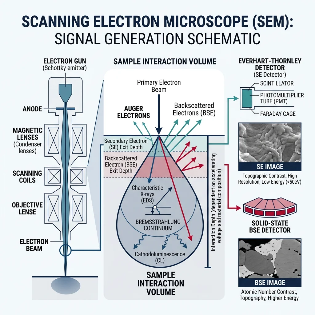
SEM Imaging Modes & Signal Types
| Signal | Detector | Information Provided | Spatial Resolution |
|---|---|---|---|
| Secondary Electrons (SE) | Everhart-Thornley | Surface topography, texture | ~1–5 nm |
| Backscattered Electrons (BSE) | Solid-state detector | Atomic number contrast (Z-contrast) | ~50–200 nm |
| Characteristic X-rays (EDS) | Silicon drift detector | Elemental composition, chemical mapping | ~1 μm interaction volume |
| Kikuchi Patterns (EBSD) | Phosphor screen + CCD | Crystal orientation, grain boundaries | ~20–50 nm |
Case Study: SEM Fractography — Turbine Blade Failure
A nickel-based superalloy turbine blade fractured after 12,000 hours of service. SEM fractography revealed three distinct zones on the fracture surface:
- Initiation Site: SE imaging showed a semi-elliptical region with transgranular facets at the blade root fillet — consistent with high-cycle fatigue initiation at a stress concentration
- Propagation Zone: Classic fatigue striations with ~0.2 μm spacing were visible, indicating stable crack growth over thousands of cycles. EDS mapping at the origin revealed elevated sulfur and chlorine — evidence of hot corrosion
- Final Overload: Dimpled rupture characteristic of ductile overload when the remaining ligament could no longer carry the load
Root Cause: Hot corrosion pitting at the blade root (from ingested sea salt) acted as a stress concentrator, initiating fatigue cracking. Recommended action: improved inlet filtration and thermal barrier coating on root fillets.
TEM & STEM
The transmission electron microscope accelerates electrons to 80–300 keV and passes them through an ultra-thin specimen (<100 nm). Because electron wavelengths at these energies are ~0.02 Å — far smaller than atomic spacings — TEM achieves sub-angstrom resolution.
TEM Imaging Modes
- Bright Field (BF): Image formed by the direct (transmitted) beam. Thicker regions and heavy atoms appear dark. Most common mode for microstructural observation
- Dark Field (DF): Image formed by selecting a specific diffracted beam with the objective aperture. Only crystallites oriented to diffract at that particular Bragg angle appear bright — powerful for identifying specific phases or precipitates
- High-Resolution TEM (HRTEM): Phase-contrast imaging using multiple beams simultaneously. Directly images the crystal lattice at atomic resolution (~0.8 Å with aberration-corrected instruments). Reveals crystal defects, interfaces, and stacking faults at the atomic scale
- Selected-Area Diffraction (SAD): An aperture selects a small region (~200 nm), and the diffraction pattern is recorded. The pattern of spots reveals crystal structure, orientation relationships, and the presence of superlattice reflections
AFM & STM
The Atomic Force Microscope (AFM) works by scanning a sharp tip (radius ~5–10 nm) mounted on a flexible cantilever across a surface. As the tip encounters surface features, the cantilever deflects. A laser reflected off the cantilever back onto a position-sensitive photodiode measures deflection with sub-angstrom precision.
AFM Operating Modes
- Contact Mode: Tip is in continuous contact; best for hard, flat surfaces. Risk of tip wear and sample damage
- Tapping Mode (Intermittent Contact): Cantilever oscillates near its resonance frequency (~300 kHz) and "taps" the surface each cycle. Reduced lateral forces — ideal for soft materials, polymers, and biological samples
- Non-Contact Mode: Tip oscillates above the surface sensing van der Waals forces. Minimal sample interaction but lower resolution
- Force Spectroscopy: Measures force vs. distance curves at individual points — quantifies adhesion, elastic modulus, and electrostatic forces at the nanoscale
Comparison: Optical Microscopy vs. SEM vs. TEM
Microscopy Technique Comparison
| Parameter | Optical Microscope | SEM | TEM | AFM |
|---|---|---|---|---|
| Resolution | ~200 nm | ~1–5 nm | ~0.5–1 Å | ~0.1 nm (Z), ~5 nm (XY) |
| Probe | Visible light | Electrons (1–30 keV) | Electrons (80–300 keV) | Physical tip |
| Sample Prep | Polish + etch | Conductive coating | Ultra-thin (<100 nm) | Minimal |
| Environment | Ambient | Vacuum | High vacuum | Ambient / liquid |
| Information | Microstructure, phases | Surface morphology, composition | Atomic structure, defects | 3D topography, forces |
| Typical Cost | $5K–$50K | $100K–$1M | $1M–$5M | $50K–$300K |
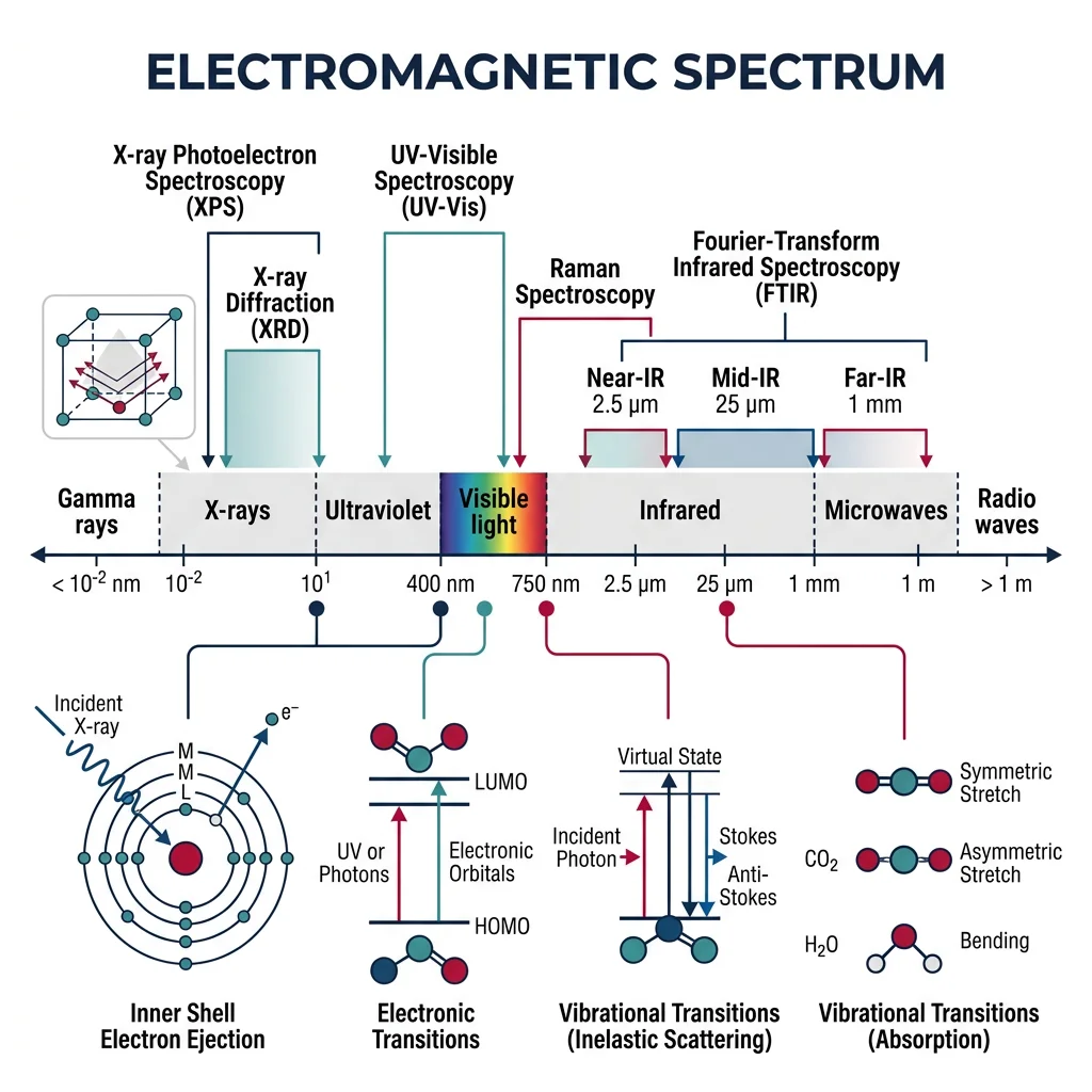
Spectroscopic Methods
While microscopy reveals where atoms are, spectroscopy tells us what atoms are present and how they are bonded. Spectroscopic techniques probe the interaction of electromagnetic radiation (or particle beams) with matter to extract chemical information.
FTIR & Raman Spectroscopy
Fourier Transform Infrared Spectroscopy (FTIR)
FTIR measures the absorption of infrared light (400–4000 cm⁻¹) by molecular vibrations. A molecule absorbs IR radiation when the vibration causes a change in dipole moment. Every functional group has characteristic absorption frequencies:
- O–H stretch: 3200–3600 cm⁻¹ (broad) — water, alcohols, carboxylic acids
- N–H stretch: 3300–3500 cm⁻¹ — amines, amides
- C–H stretch: 2850–3000 cm⁻¹ — alkanes, polymers
- C=O stretch: 1680–1750 cm⁻¹ (strong, sharp) — esters, ketones, carboxylic acids
- C=C stretch: 1600–1680 cm⁻¹ — alkenes, aromatics
- C–O stretch: 1000–1300 cm⁻¹ — ethers, esters, alcohols
- Fingerprint region: 400–1500 cm⁻¹ — unique pattern for compound identification
Raman Spectroscopy
Raman spectroscopy uses a monochromatic laser to excite the sample and measures the inelastic scattering of photons. The frequency shift equals the vibrational frequency of the molecule. Raman is complementary to FTIR because it detects vibrations with a change in polarizability rather than dipole moment:
- Symmetric vibrations (e.g., C=C, S–S) are Raman-active but IR-inactive
- Works through glass, water, and sealed containers — ideal for in-situ analysis
- Excellent for carbon materials: the D-band (~1350 cm⁻¹) and G-band (~1580 cm⁻¹) ratio quantifies defect density in graphene and carbon nanotubes
- Can map chemical composition across a surface with ~1 μm lateral resolution
Python Code: FTIR Peak Identification
import numpy as np
import matplotlib.pyplot as plt

# FTIR Peak Identification Tool
# Simulated FTIR spectrum for polyethylene terephthalate (PET)

# Wavenumber range (cm^-1)
wavenumber = np.linspace(4000, 400, 2000)

# Known PET absorption peaks and assignments
pet_peaks = {
    3440: ('O-H stretch', 'hydroxyl end groups', 15, 80),
    2960: ('C-H stretch (asym)', 'CH2 groups', 12, 50),
    2910: ('C-H stretch (sym)', 'CH2 groups', 12, 40),
    1715: ('C=O stretch', 'ester carbonyl', 10, 95),
    1580: ('C=C aromatic', 'benzene ring', 8, 35),
    1410: ('C-H bend', 'CH2 scissors', 8, 30),
    1245: ('C-O stretch (asym)', 'ester group', 10, 70),
    1096: ('C-O stretch (sym)', 'ester group', 10, 65),
    870: ('C-H out-of-plane', 'aromatic ring', 8, 40),
    725: ('C-H rock', 'aromatic ring', 8, 55),
}

# Generate simulated absorbance spectrum
absorbance = np.zeros_like(wavenumber)
for peak_pos, (assignment, group, width, intensity) in pet_peaks.items():
    absorbance += (intensity / 100) * np.exp(-0.5 * ((wavenumber - peak_pos) / width)**2)

# Add baseline noise
np.random.seed(42)
absorbance += 0.02 * np.random.randn(len(wavenumber)) + 0.05

# Plot FTIR spectrum
fig, ax = plt.subplots(figsize=(12, 5))
ax.plot(wavenumber, absorbance, 'b-', linewidth=1)
ax.set_xlim(4000, 400)
ax.set_xlabel('Wavenumber (cm$^{-1}$)', fontsize=12)
ax.set_ylabel('Absorbance (a.u.)', fontsize=12)
ax.set_title('Simulated FTIR Spectrum — PET (Polyethylene Terephthalate)', fontsize=14)

# Annotate major peaks
for peak_pos, (assignment, group, width, intensity) in pet_peaks.items():
    if intensity > 40:
        ax.annotate(f"{peak_pos}\n{assignment}",
                    xy=(peak_pos, intensity/100 + 0.06),
                    fontsize=7, ha='center', color='red',
                    arrowprops=dict(arrowstyle='->', color='red', lw=0.8))

plt.tight_layout()
plt.show()

print("\nFTIR Peak Identification Summary — PET")
print("=" * 65)
print(f"{'Wavenumber (cm⁻¹)':<20} {'Assignment':<25} {'Functional Group':<20}")
print("-" * 65)
for pos in sorted(pet_peaks.keys(), reverse=True):
    assignment, group, _, _ = pet_peaks[pos]
    print(f"{pos:<20} {assignment:<25} {group:<20}")
XPS & Auger Electron Spectroscopy
X-ray Photoelectron Spectroscopy (XPS), also known as ESCA (Electron Spectroscopy for Chemical Analysis), is the premier technique for determining surface chemical states. It works by irradiating a sample with monochromatic X-rays (typically Al Kα, 1486.6 eV) and measuring the kinetic energy of emitted photoelectrons:
Ebinding = Ephoton − Ekinetic − φ
Where φ is the spectrometer work function. The binding energy is characteristic of the element and its chemical environment. For example, carbon in a C–C bond (284.8 eV) has a different binding energy than carbon in C=O (288.5 eV) or C–F (292 eV).
Key XPS Applications
- Oxidation state analysis: Distinguish Fe⁰ vs. Fe²⁺ vs. Fe³⁺ from Fe 2p peak positions and satellite structures
- Surface contamination: Identify adventitious carbon, oxide layers, or processing residues
- Thin film composition: Quantitative elemental analysis of the top few nanometers
- Interface chemistry: Bonding at metal–oxide, polymer–metal, or catalyst–support interfaces
Mass Spectrometry & SIMS
Secondary Ion Mass Spectrometry (SIMS) bombards the sample surface with a focused primary ion beam (Cs⁺, O₂⁺, or Ga⁺), sputtering secondary ions that are analyzed by a mass spectrometer. SIMS offers parts-per-billion sensitivity for trace elements and isotopes — far exceeding EDS or XPS:
- Dynamic SIMS: High sputtering rate for depth profiling dopant distributions in semiconductors (e.g., boron implant profiles in silicon)
- Static SIMS (ToF-SIMS): Extremely low dose for surface molecular fingerprinting — identifies polymers, organic contaminants, and self-assembled monolayers
- NanoSIMS: 50 nm lateral resolution imaging of isotope distributions — used in geochemistry, biology, and nuclear materials
Thermal & In-Situ Analysis
Thermal analysis techniques measure changes in physical or chemical properties as a function of temperature. They are essential for understanding phase transitions, decomposition behavior, and processing windows for polymers, ceramics, pharmaceuticals, and metals.
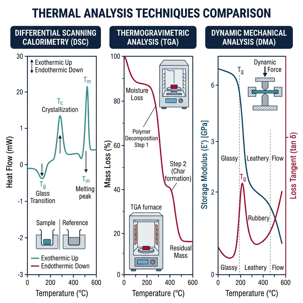
Differential Scanning Calorimetry (DSC)
DSC measures the heat flow difference between a sample and an inert reference as both are heated (or cooled) at a controlled rate. Thermal events appear as peaks or steps in the heat flow curve:
DSC Thermal Events
- Glass Transition (Tg): Step change in heat flow — amorphous regions transition from glassy to rubbery state. The midpoint of the step is reported as Tg. Endothermic direction.
- Crystallization (Tc): Exothermic peak — disordered chains or atoms organize into a crystalline lattice, releasing latent heat
- Melting (Tm): Endothermic peak — crystalline regions absorb energy to break the ordered lattice. Peak area gives the enthalpy of fusion (ΔHf), which can be used to calculate percent crystallinity
- Curing / Cross-linking: Exothermic peak — thermoset resins undergo irreversible chemical reaction. The area gives total heat of reaction
Thermogravimetric Analysis (TGA)
TGA measures the mass of a sample as it is heated in a controlled atmosphere (nitrogen, air, or argon). Mass loss steps correspond to specific decomposition, desorption, or oxidation events:
- 0–200 °C: Moisture loss, solvent evaporation
- 200–500 °C: Polymer decomposition, organic burnoff
- 500–800 °C: Carbon black oxidation (in air), carbonate decomposition (CO₂ loss)
- Residue at 800+ °C: Inorganic filler content (glass fiber, mineral fillers, metals)
Case Study: Identifying an Unknown Polymer with DSC + TGA
An unknown white plastic pellet was submitted for identification. Combining DSC and TGA provided a definitive answer:
- DSC (1st heating, 10 °C/min in N₂): No glass transition observed → highly crystalline polymer. Sharp melting endotherm at Tm = 163 °C with ΔHf = 95 J/g → crystallinity ~46%. Cold crystallization peak at 125 °C on cooling confirmed semi-crystalline nature.
- TGA (10 °C/min in N₂): Single-step decomposition onset at 420 °C, complete by 500 °C. Residue: 0.3% → no significant inorganic filler.
- Identification: Tm of 163 °C and decomposition above 400 °C are characteristic of isotactic polypropylene (iPP). Cross-reference with FTIR (C–H stretching at 2950 cm⁻¹, CH₃ deformation at 1375 cm⁻¹) confirmed the identification.
This three-technique workflow (DSC → TGA → FTIR) is the standard approach for unknown polymer identification in industrial and forensic labs.
Dynamic Mechanical Analysis (DMA)
DMA applies an oscillating stress (or strain) to a sample while varying temperature and measures the material's viscoelastic response. The key outputs are:
- Storage Modulus (E'): The elastic (in-phase) component — represents energy stored and recovered per cycle. Measures stiffness.
- Loss Modulus (E''): The viscous (out-of-phase) component — represents energy dissipated as heat per cycle. Measures damping.
- tan δ = E''/E': The loss tangent — ratio of energy dissipated to energy stored. The peak in tan δ corresponds to the glass transition temperature, often used for Tg determination in composites and coatings.
Python Code: DSC Curve Simulation
import numpy as np
import matplotlib.pyplot as plt

# Simulate a DSC curve for a semi-crystalline polymer (e.g., PET)
# Shows glass transition, cold crystallization, and melting

temperature = np.linspace(30, 300, 1000)  # Temperature range in °C
heat_flow = np.zeros_like(temperature)

# 1. Glass transition (Tg ~ 80°C) — step change in heat flow
Tg = 80
tg_width = 8
heat_flow += 0.15 / (1 + np.exp(-(temperature - Tg) / tg_width))

# 2. Cold crystallization (Tc ~ 130°C) — exothermic peak (negative by convention)
Tc = 130
tc_width = 6
dH_c = -2.5  # J/g (exothermic = negative)
heat_flow += dH_c * np.exp(-0.5 * ((temperature - Tc) / tc_width)**2) / (tc_width * np.sqrt(2 * np.pi)) * 15

# 3. Melting (Tm ~ 255°C) — endothermic peak (positive)
Tm = 255
tm_width = 5
dH_m = 4.0  # J/g (endothermic = positive)
heat_flow += dH_m * np.exp(-0.5 * ((temperature - Tm) / tm_width)**2) / (tm_width * np.sqrt(2 * np.pi)) * 15

# 4. Add baseline slope (instrumental drift)
heat_flow += 0.001 * (temperature - 30)

# Add small noise for realism
np.random.seed(42)
heat_flow += 0.005 * np.random.randn(len(temperature))

# Plot DSC curve
fig, ax = plt.subplots(figsize=(10, 6))
ax.plot(temperature, heat_flow, 'b-', linewidth=1.5)
ax.set_xlabel('Temperature (°C)', fontsize=12)
ax.set_ylabel('Heat Flow (W/g)     Endo ↑', fontsize=12)
ax.set_title('Simulated DSC Curve — PET (Polyethylene Terephthalate)', fontsize=14)

# Annotate thermal events
ax.annotate('Glass Transition\nTg ≈ 80 °C', xy=(80, 0.08), xytext=(40, 0.25),
            fontsize=10, ha='center', color='green',
            arrowprops=dict(arrowstyle='->', color='green', lw=1.5))
ax.annotate('Cold Crystallization\nTc ≈ 130 °C', xy=(130, -0.12), xytext=(100, -0.28),
            fontsize=10, ha='center', color='purple',
            arrowprops=dict(arrowstyle='->', color='purple', lw=1.5))
ax.annotate('Melting\nTm ≈ 255 °C', xy=(255, 0.35), xytext=(270, 0.45),
            fontsize=10, ha='center', color='red',
            arrowprops=dict(arrowstyle='->', color='red', lw=1.5))

ax.axhline(y=0, color='gray', linestyle='--', linewidth=0.5)
plt.tight_layout()
plt.show()

print("DSC Thermal Events Summary:")
print(f"  Glass Transition (Tg): ~{Tg} °C")
print(f"  Cold Crystallization (Tc): ~{Tc} °C (exothermic)")
print(f"  Melting (Tm): ~{Tm} °C (endothermic)")
In-Situ Characterization
Traditional characterization examines materials after processing ("post-mortem"). In-situ techniques observe materials during processing or testing, capturing transient states that would otherwise be missed:
- In-situ XRD: Track phase transformations during heating/cooling — watch austenite transform to martensite in real time. Synchrotron sources enable sub-second time resolution
- In-situ TEM: Observe dislocation motion, crack propagation, and nanoparticle growth while applying stress, heat, or electrical bias inside the microscope
- In-situ SEM/EBSD: Map grain rotation and texture evolution during tensile testing — connect macroscopic stress-strain behavior to mesoscale deformation mechanisms
- Synchrotron techniques: High-brilliance X-ray sources enable time-resolved SAXS/WAXS during polymer crystallization, operando studies of battery electrodes, and 3D non-destructive tomography
AI-Assisted Characterization
Machine learning is transforming materials characterization by automating tasks that traditionally required expert human interpretation:
- Automated Phase Identification: Convolutional neural networks (CNNs) match XRD patterns to crystal structures, achieving >95% accuracy across databases of 100,000+ phases
- Microstructure Segmentation: U-Net and similar architectures segment SEM/TEM images into phases, grains, and defects with pixel-level precision — replacing hours of manual annotation
- Spectrum Deconvolution: Machine learning decomposes overlapping XPS or Raman peaks more objectively than manual curve fitting, reducing analyst bias
- Autonomous Experiments: AI-driven microscopes that decide where to look next based on what they've already seen — maximizing information gain per measurement
Technique Comparison Guide
The following table provides a comprehensive reference for selecting the right characterization technique based on information needed, sample requirements, and practical constraints:
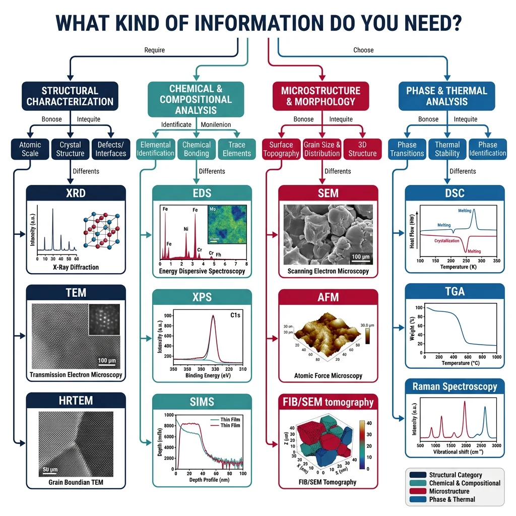
Comprehensive Characterization Techniques Comparison
| Technique | What It Measures | Resolution / Sensitivity | Sample Requirement | Best For |
|---|---|---|---|---|
| XRD | Crystal structure, phases, lattice parameters | Phase detection ~1–5 wt% | Powder or flat solid | Phase ID, crystallinity |
| SEM | Surface morphology, Z-contrast, composition (EDS) | ~1–5 nm spatial | Conductive surface | Fracture surfaces, microstructure |
| TEM | Atomic structure, defects, diffraction | ~0.5 Å (aberration-corrected) | Ultra-thin foil (<100 nm) | Precipitates, interfaces, atomic imaging |
| AFM | 3D surface topography, mechanical properties | ~0.1 nm (Z), ~5 nm (XY) | Flat surface, any material | Thin films, polymers, biological |
| XPS | Surface elemental composition, chemical states | ~0.1 at%, top 5–10 nm | Solid surface (vacuum compatible) | Oxidation states, surface chemistry |
| FTIR | Molecular bonds, functional groups | ~1 wt% (bulk); monolayer (ATR) | Solid, liquid, gas, thin film | Polymer ID, organic analysis |
| Raman | Molecular vibrations, crystal symmetry | ~1 μm spatial; ~1 wt% | Any (through glass/water) | Carbon materials, in-situ analysis |
| DSC | Thermal transitions (Tg, Tm, Tc), enthalpies | ~0.01 W/g sensitivity | 5–20 mg solid or powder | Polymer characterization, phase transitions |
| TGA | Mass change vs. temperature | ~0.1 μg balance resolution | 5–50 mg any form | Decomposition, filler content |
| DMA | Viscoelastic properties (E', E'', tan δ) | Modulus range 10⁴–10¹² Pa | Bar, film, or fiber specimen | Polymer Tg, composite performance |
| SIMS | Trace elements, isotope ratios, depth profiles | ppb sensitivity; 50 nm lateral | Solid surface (vacuum) | Dopant profiling, contamination |
| EBSD | Crystal orientation, grain boundaries, texture | ~20–50 nm; <0.5° angular | Polished flat surface | Grain mapping, deformation studies |
Practice Exercises
Exercise 1: Bragg's Law Calculation
An XRD pattern of an FCC aluminum sample (Cu Kα radiation, λ = 1.5406 Å) shows its first diffraction peak at 2θ = 38.47°. Calculate:
- The d-spacing for this peak
- The Miller indices (hkl) of this reflection (hint: the first allowed reflection for FCC is (111))
- The lattice parameter a of aluminum
- Compare your calculated a to the literature value (4.0495 Å) — what is the percent error?
Exercise 2: Choosing the Right Technique
For each scenario below, identify the best primary characterization technique and justify your choice:
- You need to determine whether a stainless steel weld contains sigma phase (an intermetallic compound)
- A silicon wafer has been implanted with boron ions — you need the concentration-depth profile
- You suspect a polymer automotive part failed due to UV degradation — you want to check for chain scission and carbonyl formation on the surface
- You need to measure the grain size distribution and texture of a rolled copper sheet
- An unknown white powder may be a pharmaceutical compound or an illicit substance — rapid, non-destructive identification is needed
Exercise 3: DSC Interpretation
A DSC scan of an unknown polymer shows the following features during heating at 10 °C/min:
- Step change in heat flow at 105 °C
- Exothermic peak centered at 165 °C
- Endothermic peak centered at 265 °C
- Identify each thermal event (glass transition, crystallization, melting, or curing)
- Is this a semi-crystalline or amorphous polymer? How do you know?
- Based on the Tg and Tm values, suggest a candidate polymer (hint: consider PET, nylon 6,6, or polycarbonate)
Exercise 4: SEM vs. TEM Decision Tree
You're investigating a new nickel superalloy with γ' precipitates expected to be ~20 nm in diameter:
- Can you resolve the precipitates using SEM? Why or why not?
- What TEM imaging mode would best reveal the precipitates?
- How would you prepare a TEM sample from a bulk alloy specimen?
- If you also need to confirm the precipitate crystal structure, what TEM technique would you use?
Exercise 5: FTIR Functional Group Analysis
An FTIR spectrum of a clear coating shows strong absorption bands at the following wavenumbers:
- 3340 cm⁻¹ (broad)
- 2930 cm⁻¹ and 2860 cm⁻¹
- 1730 cm⁻¹ (strong, sharp)
- 1240 cm⁻¹ and 1050 cm⁻¹
- Assign each absorption band to a functional group
- What type of polymer does this spectrum suggest? (hint: polyurethane, polyester, or polyacrylate)
- The coating was exposed to 500 hours of UV aging. You observe the 1730 cm⁻¹ peak broaden and a new peak appears at 1660 cm⁻¹. What degradation mechanism do these changes suggest?
Exercise 6: Coding Challenge — Scherrer Equation
Write a Python script that:
- Accepts three XRD peak FWHM values (in degrees) at three different 2θ positions
- Applies the Scherrer equation (τ = Kλ / β cos θ) with K = 0.9 and λ = 1.5406 Å
- Reports the average crystallite size in nanometers
- Creates a Williamson-Hall plot (β cos θ vs. 4 sin θ) and determines if peak broadening is dominated by size or strain
Hint: Convert FWHM from degrees to radians before using the Scherrer equation. Subtract instrumental broadening (~0.05°) from measured FWHM.
Conclusion & Next Steps
Materials characterization is the bridge between theory and practice — without it, we cannot validate computational predictions, diagnose failures, or develop new materials with confidence. In this guide, we explored the full characterization toolkit:
- Diffraction techniques (XRD, neutron, EBSD) reveal crystal structure, phase composition, and texture
- Electron microscopy (SEM, TEM) provides morphological and atomic-scale structural information
- Surface & spectroscopic methods (XPS, FTIR, Raman, SIMS) identify chemical bonding and composition
- Thermal analysis (DSC, TGA, DMA) quantifies phase transitions and processing behavior
- In-situ and AI-assisted methods are pushing characterization toward real-time, autonomous operation
The most powerful approach is multi-technique characterization — combining complementary methods to build a complete picture of a material's structure, chemistry, and properties. No single technique tells the whole story, but together they provide the comprehensive understanding needed for materials design and engineering.