Semiconductor Materials
Materials Science Mastery
Atomic Structure & Quantum Foundations
Quantum mechanics, bonding, band theory, Fermi energy, phononsCrystal Structures, Defects & Diffusion
FCC/BCC/HCP, Miller indices, dislocations, phase diagrams, Fick's lawsMetals & Alloys
Iron-carbon diagram, steels, aluminum, titanium, superalloys, heat treatmentPolymers & Soft Materials
Polymer chemistry, thermoplastics, viscoelasticity, rheology, biopolymersCeramics, Glass & Composites
Oxide ceramics, toughening, fiber-reinforced composites, interfacial bondingMechanical Behavior & Testing
Stress-strain, hardness, fatigue, fracture toughness, nanoindentationFailure Analysis & Reliability Engineering
Fractography, corrosion, tribology, root cause analysisNanomaterials & Smart Materials
Nanotubes, graphene, piezoelectrics, shape memory alloys, self-healingMaterials Characterization Techniques
XRD, SEM, TEM, AFM, DSC, TGA, spectroscopyThermodynamics & Kinetics of Materials
Gibbs free energy, CALPHAD, phase stability, solidificationElectronic, Magnetic & Optical Materials
Semiconductors, photovoltaics, dielectrics, superconductorsBiomaterials
Implants, biocompatibility, tissue engineering, drug deliveryEnergy Materials
Battery materials, hydrogen storage, fuel cells, nuclear materialsComputational Materials Science
DFT, molecular dynamics, FEM, materials informatics, AIBand Theory: Conductors, Semiconductors & Insulators
Every solid has electrons arranged in energy bands — continuous ranges of allowed quantum states. The two most important bands are the valence band (filled with electrons at $T = 0$ K) and the conduction band (empty at $T = 0$ K). The energy gap between them — the band gap ($E_g$) — determines whether a material conducts, insulates, or semiconducts.
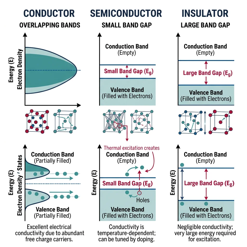
Quantitatively, materials are classified by their band gap:
| Category | Band Gap ($E_g$) | Examples | Conductivity (S/m) |
|---|---|---|---|
| Conductor | 0 eV (overlapping bands) | Cu, Al, Ag, Au | $10^6 – 10^8$ |
| Semiconductor | 0.1 – 4 eV | Si (1.1 eV), GaAs (1.4 eV), GaN (3.4 eV) | $10^{-6} – 10^4$ |
| Insulator | > 4 eV | SiO₂ (9 eV), Diamond (5.5 eV), Al₂O₃ (8.8 eV) | $< 10^{-10}$ |
Intrinsic vs Extrinsic Semiconductors: Doping
An intrinsic semiconductor is a pure crystal (e.g., ultra-pure Si) where conduction relies solely on thermally generated electron-hole pairs. At room temperature, intrinsic Si has roughly $n_i \approx 1.5 \times 10^{10}$ carriers/cm³ — tiny compared to copper's $\sim 10^{22}$/cm³.
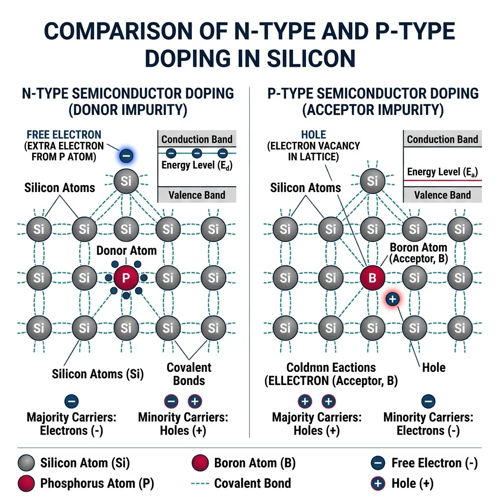
To make semiconductors useful, we intentionally add impurities — a process called doping:
- n-type doping: Adding a Group V element (P, As, Sb) to Si donates an extra electron per atom. These donor atoms create occupied states just below the conduction band, dramatically increasing electron concentration.
- p-type doping: Adding a Group III element (B, Ga, In) creates an electron deficit — a hole — per atom. These acceptor atoms create empty states just above the valence band, increasing hole concentration.
Python: Fermi-Dirac Distribution Visualization
import numpy as np
import matplotlib.pyplot as plt

# Energy range relative to Fermi level (eV)
E = np.linspace(-0.5, 0.5, 500)
Ef = 0.0           # Fermi energy (eV)
kB = 8.617e-5       # Boltzmann constant (eV/K)

# Fermi-Dirac distribution at different temperatures
temperatures = [100, 300, 600, 1200]  # Kelvin
colors = ['#132440', '#16476A', '#3B9797', '#BF092F']

plt.figure(figsize=(9, 6))
for T, color in zip(temperatures, colors):
    f_E = 1.0 / (1.0 + np.exp((E - Ef) / (kB * T)))
    plt.plot(E, f_E, linewidth=2.5, label=f'T = {T} K', color=color)

# Step function at T = 0 K for reference
plt.step([-0.5, 0, 0, 0.5], [1, 1, 0, 0], linewidth=1.5,
         linestyle='--', color='gray', label='T = 0 K (ideal)')

plt.xlabel('Energy − E_F (eV)', fontsize=13)
plt.ylabel('f(E) — Occupation Probability', fontsize=13)
plt.title('Fermi-Dirac Distribution at Various Temperatures', fontsize=14)
plt.legend(fontsize=11)
plt.grid(True, alpha=0.3)
plt.axhline(y=0.5, color='gray', linestyle=':', alpha=0.5)
plt.axvline(x=0.0, color='gray', linestyle=':', alpha=0.5)
plt.tight_layout()
plt.show()
print("At T=300K, f(E_F + 0.1 eV) =", round(1/(1+np.exp(0.1/(kB*300))), 4))
print("At T=300K, f(E_F - 0.1 eV) =", round(1/(1+np.exp(-0.1/(kB*300))), 4))
P-N Junctions & Devices
When a p-type region meets an n-type region in a single crystal, the interface forms a p-n junction — the fundamental building block of all semiconductor devices: diodes, transistors, LEDs, solar cells, and lasers.
At the junction, electrons from the n-side diffuse into the p-side (and holes diffuse the opposite way). This leaves behind fixed ionized donors (positive) on the n-side and ionized acceptors (negative) on the p-side, creating a depletion region with a built-in electric field that opposes further diffusion. The resulting built-in voltage for Si is typically $V_{bi} \approx 0.6–0.7$ V.
Key p-n junction device applications:
- Rectifier diodes: Convert AC to DC by allowing current in one direction only
- Zener diodes: Operate in controlled reverse breakdown for voltage regulation
- LEDs: Forward-biased junctions in direct-bandgap semiconductors emit photons when electrons recombine with holes
- Solar cells: Photons generate electron-hole pairs in the depletion region; the built-in field separates them, producing current
- Transistors (BJT): Two back-to-back p-n junctions enabling amplification and switching
Photovoltaic Materials & Optoelectronics
Solar Cell Physics
A solar cell converts sunlight into electricity through three steps:
- Photon absorption: A photon with energy $E_{photon} = h\nu \geq E_g$ is absorbed, promoting an electron from the valence band to the conduction band and creating an electron-hole pair.
- Carrier generation & transport: The photo-generated carriers diffuse toward the p-n junction. Carriers generated within the depletion region (or within a diffusion length of it) are swept across by the built-in electric field.
- Carrier separation & collection: The internal field separates electrons (pushed to n-side) from holes (pushed to p-side), generating a photovoltage and photocurrent collected by metal contacts.
LED Materials
LEDs require direct band gap semiconductors (where electrons can recombine with holes without needing a phonon). Key material systems:
- GaN / InGaN: Blue and white LEDs (Shuji Nakamura, 2014 Nobel Prize). Blue LEDs + yellow phosphor coating = white light. Band gap tunable from 0.7 eV (InN) to 3.4 eV (GaN).
- InGaAlP: Red, orange, and yellow LEDs. Lattice-matched to GaAs substrates for high efficiency.
- GaAs / AlGaAs: Infrared LEDs and laser diodes. Used in fiber-optic communication (850 nm).
Case Study: Perovskite Solar Cells — A Disruptive Technology
What: Metal-halide perovskites (general formula ABX₃, e.g., CH₃NH₃PbI₃ or "MAPI") have seen their power conversion efficiency skyrocket from 3.8% in 2009 to over 26% in 2024 — the fastest improvement of any solar technology in history.
Why they're exciting:
- Solution-processable — can be spin-coated or printed at low temperature (~100°C vs ~1400°C for Si)
- Tunable band gap (1.2–2.3 eV) by adjusting halide composition (I, Br, Cl mixing)
- Excellent absorption coefficient (~10× higher than Si)
- Cost potential: $<$0.20/W vs ~$0.30/W for crystalline Si
Remaining challenges: Long-term stability (moisture, heat, UV degradation), lead toxicity concerns (Pb content), and scaling from lab cells (1 cm²) to commercial modules (m²). Encapsulation and tin-based lead-free alternatives are active research fronts.
Solar Cell Technology Comparison
| Technology | Band Gap (eV) | Record η (%) | Commercial η (%) | Key Advantage | Key Limitation |
|---|---|---|---|---|---|
| Crystalline Si | 1.12 | 26.8 | 20–22 | Mature, abundant, reliable | Indirect gap, rigid, energy-intensive mfg |
| GaAs | 1.42 | 29.1 | 28–29 | Highest single-junction η, radiation-tolerant | Extremely expensive ($100+/W), Ga scarcity |
| CdTe | 1.45 | 22.1 | 18–19 | Low manufacturing cost, thin film | Cd toxicity, Te scarcity |
| Perovskite | 1.2–2.3 (tunable) | 26.1 | Emerging | Low-cost processing, tunable gap, tandem-ready | Stability, lead content, scalability |
| Perovskite/Si Tandem | 1.7 / 1.12 stack | 33.9 | Emerging | Exceeds Shockley-Queisser limit | Complex fabrication, early-stage |
Magnetic Materials
Types of Magnetism
All materials respond to external magnetic fields, but the nature and strength of that response varies enormously. The magnetic behavior depends on the arrangement of electron spins and orbital angular momenta:
| Type | Susceptibility ($\chi$) | Spin Alignment | Examples |
|---|---|---|---|
| Diamagnetic | Small, negative ($\sim -10^{-5}$) | No unpaired electrons; weakly opposes applied field | Cu, Au, Si, H₂O, most organics |
| Paramagnetic | Small, positive ($\sim 10^{-3}$) | Random unpaired spins; weakly aligns with field | Al, Pt, O₂, Mn²⁺ salts |
| Ferromagnetic | Very large, positive ($\sim 10^2 – 10^5$) | Parallel alignment in domains; strong permanent magnets | Fe, Co, Ni, Nd₂Fe₁₄B |
| Antiferromagnetic | Small, positive | Adjacent spins antiparallel; net magnetization ≈ 0 | MnO, Cr, NiO, FeO |
| Ferrimagnetic | Large, positive | Antiparallel but unequal spins; net magnetization ≠ 0 | Fe₃O₄ (magnetite), ferrites |
Hysteresis Loops: Coercivity, Remanence & Saturation
When a ferromagnetic material is subjected to a cyclic external magnetic field $H$, its magnetization $B$ (or $M$) traces out a characteristic hysteresis loop. Three critical parameters define this loop:
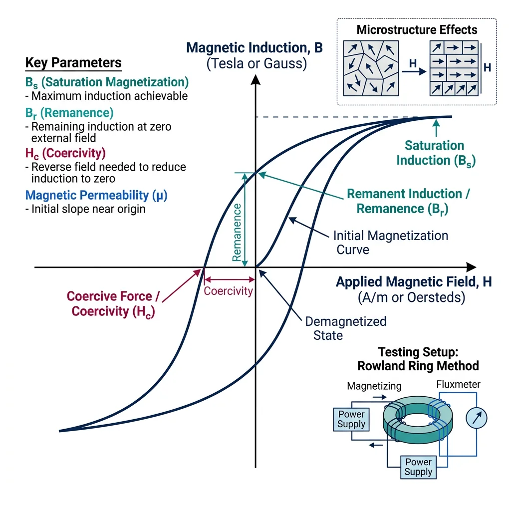
- Saturation magnetization ($B_s$): The maximum magnetization when all domains are fully aligned. For pure iron, $B_s \approx 2.16$ T.
- Remanence ($B_r$): The residual magnetization remaining after the external field is removed. High $B_r$ means a strong permanent magnet.
- Coercivity ($H_c$): The reverse field strength required to demagnetize the material (drive $B$ to zero). High $H_c$ means the magnet is "hard" to demagnetize.
Hard vs Soft Magnets
| Property | Soft Magnets | Hard (Permanent) Magnets |
|---|---|---|
| Coercivity | Low ($H_c < 1$ kA/m) | High ($H_c > 100$ kA/m) |
| Hysteresis loop | Narrow (low energy loss per cycle) | Wide (stores energy as permanent field) |
| Examples | Pure Fe, Si-Fe steel, Ni-Fe permalloy, ferrites | Nd₂Fe₁₄B, SmCo₅, Alnico, Ba/Sr ferrites |
| Applications | Transformer cores, inductors, electromagnetic shielding | Electric motors, speakers, MRI scanners, wind turbines |
Python: B-H Hysteresis Loop Simulation
import numpy as np
import matplotlib.pyplot as plt

# Simulate a B-H hysteresis loop using a simple arctangent model
# Parameters for a hard magnet (Nd2Fe14B-like)
Bs = 1.3          # Saturation magnetization (T)
Br = 1.2          # Remanence (T)
Hc = 900           # Coercivity (kA/m)

# Generate H field cycle: 0 -> +Hmax -> -Hmax -> +Hmax
Hmax = 1500        # kA/m
N = 1000
H_up = np.linspace(0, Hmax, N)
H_down = np.linspace(Hmax, -Hmax, 2 * N)
H_back = np.linspace(-Hmax, Hmax, 2 * N)

# Arctangent hysteresis model
def B_upper(H, Bs, Hc, Br):
    """Upper branch of hysteresis loop."""
    return Bs * np.tanh((H + Hc * 0.6) / (Hc * 0.8))

def B_lower(H, Bs, Hc, Br):
    """Lower branch of hysteresis loop."""
    return Bs * np.tanh((H - Hc * 0.6) / (Hc * 0.8))

H_full = np.linspace(-Hmax, Hmax, N)
B_up = B_upper(H_full, Bs, Hc, Br)
B_low = B_lower(H_full, Bs, Hc, Br)

# Also simulate a soft magnet (Si-steel-like)
Bs_soft, Hc_soft = 2.0, 50
B_up_soft = Bs_soft * np.tanh((H_full + Hc_soft * 0.6) / (Hc_soft * 0.8))
B_low_soft = Bs_soft * np.tanh((H_full - Hc_soft * 0.6) / (Hc_soft * 0.8))

fig, axes = plt.subplots(1, 2, figsize=(14, 6))

# Hard magnet
axes[0].plot(H_full, B_up, color='#BF092F', linewidth=2.5, label='Upper branch')
axes[0].plot(H_full, B_low, color='#132440', linewidth=2.5, label='Lower branch')
axes[0].fill_between(H_full, B_low, B_up, alpha=0.08, color='#BF092F')
axes[0].axhline(0, color='gray', linewidth=0.5)
axes[0].axvline(0, color='gray', linewidth=0.5)
axes[0].set_xlabel('H (kA/m)', fontsize=12)
axes[0].set_ylabel('B (T)', fontsize=12)
axes[0].set_title('Hard Magnet (Nd₂Fe₁₄B-type)', fontsize=13)
axes[0].annotate('Br', xy=(0, Br), fontsize=11, color='#BF092F',
                 xytext=(200, Br+0.15), arrowprops=dict(arrowstyle='->', color='#BF092F'))
axes[0].annotate('-Hc', xy=(-Hc, 0), fontsize=11, color='#132440',
                 xytext=(-Hc-300, 0.4), arrowprops=dict(arrowstyle='->', color='#132440'))
axes[0].legend(fontsize=10)
axes[0].grid(True, alpha=0.3)

# Soft magnet
axes[1].plot(H_full, B_up_soft, color='#3B9797', linewidth=2.5, label='Upper branch')
axes[1].plot(H_full, B_low_soft, color='#16476A', linewidth=2.5, label='Lower branch')
axes[1].fill_between(H_full, B_low_soft, B_up_soft, alpha=0.08, color='#3B9797')
axes[1].axhline(0, color='gray', linewidth=0.5)
axes[1].axvline(0, color='gray', linewidth=0.5)
axes[1].set_xlabel('H (kA/m)', fontsize=12)
axes[1].set_ylabel('B (T)', fontsize=12)
axes[1].set_title('Soft Magnet (Si-Steel-type)', fontsize=13)
axes[1].legend(fontsize=10)
axes[1].grid(True, alpha=0.3)

plt.tight_layout()
plt.show()
print(f"Hard magnet — Bs: {Bs} T, Br: {Br} T, Hc: {Hc} kA/m")
print(f"Soft magnet — Bs: {Bs_soft} T, Hc: {Hc_soft} kA/m")
print(f"Energy product proxy (BH_max ~ Br*Hc): {Br * Hc:.0f} kJ/m³")
Case Study: Nd₂Fe₁₄B Rare Earth Magnets in EV Motors
Context: Neodymium-iron-boron (Nd₂Fe₁₄B) magnets, discovered in 1984 by Sagawa (Sumitomo) and Croat (GM), are the strongest permanent magnets ever made. With an energy product $(BH)_{max}$ exceeding 400 kJ/m³ — roughly 10× that of traditional ferrite magnets — they enable compact, lightweight, high-torque electric motors.
EV motor application: A typical Tesla Model 3 permanent-magnet synchronous motor contains ~1–2 kg of Nd₂Fe₁₄B magnets arranged in a Halbach array configuration in the rotor. These magnets produce a powerful radial field that interacts with the stator's electromagnetic coils, achieving peak efficiencies >97%.
Materials challenges:
- Temperature sensitivity: Nd₂Fe₁₄B begins to demagnetize above ~150°C. Adding dysprosium (Dy) or terbium (Tb) to the grain boundaries improves thermal stability but increases cost and supply chain risk.
- Supply concentration: China produces ~60% of rare earth minerals and ~90% of processed rare earth magnets, creating geopolitical vulnerability.
- Recycling gap: Less than 1% of rare earth magnets are currently recycled. Research into hydrogen decrepitation and acid-free recycling aims to close this loop.
Alternatives under development: Ferrite-assisted PM motors, Ce-substituted magnets, and advanced wound-rotor synchronous machines that eliminate rare earths entirely.
Spintronics & GMR
Spintronics (spin electronics) exploits the intrinsic spin of electrons — in addition to their charge — to store, process, and transmit information. The breakthrough that launched the field was Giant Magnetoresistance (GMR), discovered independently by Albert Fert and Peter Grünberg in 1988 (2007 Nobel Prize in Physics).
In a GMR device, thin alternating layers of ferromagnetic and non-magnetic metals (e.g., Fe/Cr/Fe) show dramatically different electrical resistance depending on whether the magnetization in adjacent ferromagnetic layers is parallel (low resistance) or antiparallel (high resistance). This resistance change can exceed 50% — hence "giant."
Dielectric & Insulating Materials
Dielectric Properties & Permittivity
A dielectric material is an electrical insulator that can be polarized by an applied electric field. Unlike conductors, charges in dielectrics don't flow — instead, they shift slightly (electronic, ionic, or orientational polarization), creating internal electric dipoles that partially oppose the applied field.
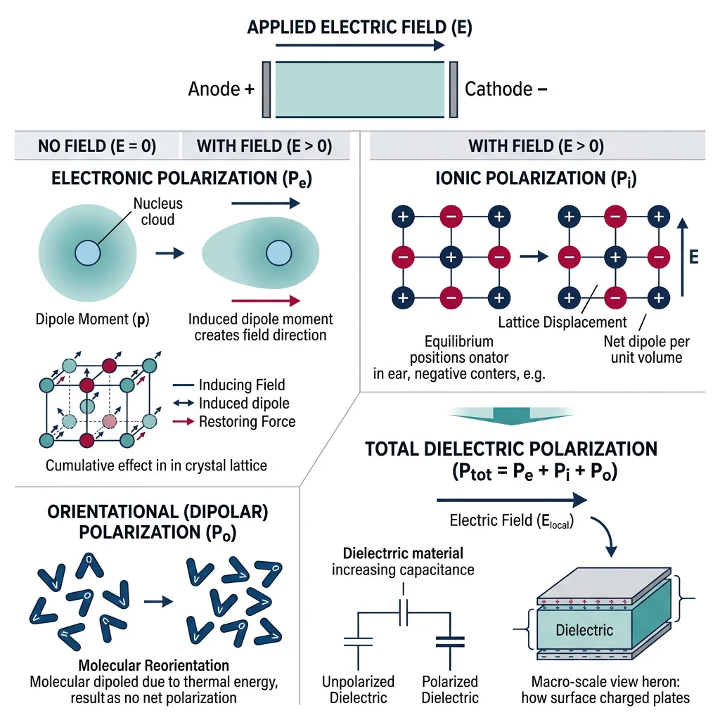
The key property is the relative permittivity (dielectric constant) $\kappa = \varepsilon_r = \varepsilon / \varepsilon_0$, which measures how effectively a material stores electrical energy. A parallel-plate capacitor with a dielectric has capacitance:
$$C = \kappa \varepsilon_0 \frac{A}{d}$$
where $A$ is the plate area, $d$ is the separation, and $\varepsilon_0 = 8.854 \times 10^{-12}$ F/m. Inserting a dielectric with $\kappa = 25$ (e.g., HfO₂) increases capacitance by 25× compared to vacuum.
High-k & Low-k Dielectrics in Microelectronics
Two opposite trends drive dielectric research in chip manufacturing:
Low-k dielectrics: Between metal interconnect wires, low permittivity ($\kappa < 3$) is needed to minimize parasitic capacitance and RC delay. Materials include SiCOH ($\kappa \approx 2.5–3.0$), porous organosilicates ($\kappa \approx 2.0–2.5$), and air gaps ($\kappa = 1$). The tradeoff: lower $\kappa$ materials are mechanically weaker and harder to process.
Piezoelectric & Ferroelectric Materials
Piezoelectric materials generate an electric charge when mechanically stressed (direct effect) or deform when an electric field is applied (converse effect). Key materials include quartz (SiO₂), PZT (Pb(Zr,Ti)O₃), and AlN. Applications span pressure sensors, ultrasonic transducers, MEMS actuators, and quartz oscillator clocks.
Ferroelectric materials are a subset of piezoelectrics that exhibit a spontaneous electric polarization that can be reversed by an applied field — the electrical analogue of ferromagnetic hysteresis. Key examples: BaTiO₃, PZT, and HfO₂-based films (used in FeRAM nonvolatile memory). The Curie temperature $T_C$ marks the transition from ferroelectric to paraelectric behavior (BaTiO₃: $T_C = 120°C$).
Superconductors
Below a critical temperature $T_c$, certain materials exhibit exactly zero electrical resistance and expel magnetic fields from their interior (Meissner effect). This is not merely low resistance — it is a fundamentally different quantum state of matter.
BCS Theory & Cooper Pairs
The BCS theory (Bardeen, Cooper, Schrieffer — 1957 Nobel Prize) explains conventional superconductivity: at low temperatures, electrons form Cooper pairs — bound pairs of electrons with opposite spin and momentum, mediated by phonon interactions with the crystal lattice. These pairs condense into a macroscopic quantum state (a Bose-Einstein condensate of pairs) that can flow without scattering. The energy gap $2\Delta$ required to break a Cooper pair is typically $\sim 1$ meV.
Type I vs Type II Superconductors
| Property | Type I | Type II |
|---|---|---|
| Meissner effect | Complete — abrupt transition | Partial — flux vortices penetrate above $H_{c1}$ |
| Critical field | Single $H_c$ (low, typically < 0.1 T) | Two fields: $H_{c1}$ and $H_{c2}$ (can exceed 100 T) |
| $T_c$ range | < 10 K | Up to 138 K (HgBaCaCuO), room T under extreme pressure |
| Examples | Hg (4.2 K), Pb (7.2 K), Al (1.2 K) | NbTi (9.8 K), Nb₃Sn (18 K), YBCO (92 K), MgB₂ (39 K) |
| Key applications | Limited (low fields) | MRI magnets, particle accelerators, power cables, maglev |
Case Study: YBCO Superconducting Power Cables
Material: YBa₂Cu₃O₇₋ₓ (YBCO) — a Type II high-temperature superconductor with $T_c \approx 92$ K, above liquid nitrogen's boiling point (77 K). This was revolutionary because liquid nitrogen is cheap (~$0.50/liter vs ~$5/liter for liquid helium) and widely available.
Project — AmpaCity (Essen, Germany, 2014): The world's longest superconducting power cable (1 km) was installed in downtown Essen, replacing a 110 kV overhead line with a 10 kV YBCO cable. Results:
- Carried 40 MW through a cable just 15 cm in diameter — a conventional cable would need 5× the cross-section
- Zero resistive losses (only cooling energy required: ~10 W/m)
- Eliminated the need for bulky 110 kV/10 kV transformers in the city center
- CO₂ reduction: ~1,000 tonnes/year compared to conventional copper cables
Challenge: Maintaining cryogenic temperatures requires continuous LN₂ circulation. Fault current limiting (built into YBCO cables — they quench and become resistive under overcurrent) adds an inherent safety feature.
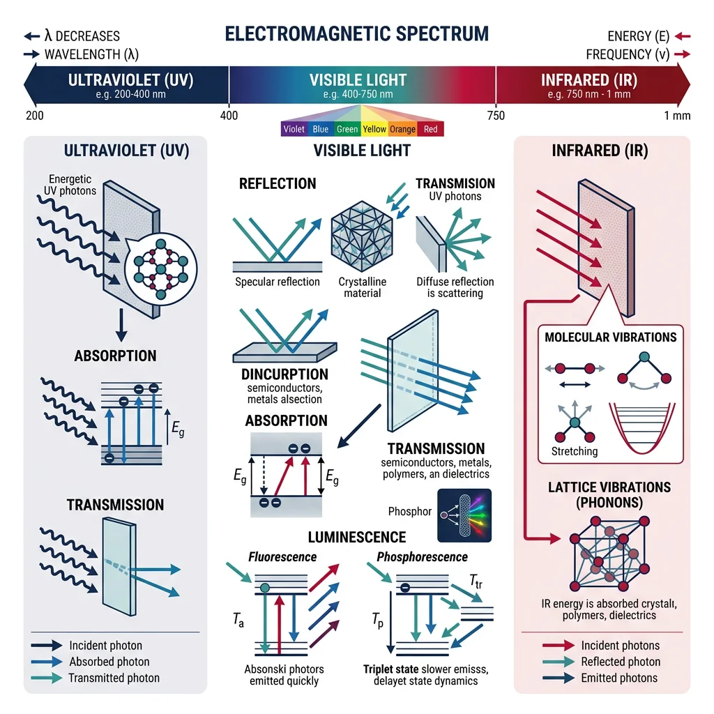
Optical & Photonic Materials
Optical materials interact with electromagnetic radiation across the spectrum — from UV through visible to infrared. The key phenomena are absorption, transmission, reflection, refraction, and luminescence (fluorescence and phosphorescence).
A material's optical behavior is governed by its complex refractive index $\tilde{n} = n + ik$, where $n$ is the real refractive index (how much light slows down) and $k$ is the extinction coefficient (how much light is absorbed). For window glass, $n \approx 1.5$ and $k \approx 0$ in the visible range — highly transparent. For metals, $k$ is large — they are opaque and reflective.
LED & Laser Materials in Depth
Modern LEDs have transformed lighting — a white LED converts ~50% of electrical energy to light (vs ~5% for incandescent bulbs). The efficiency metric is luminous efficacy, measured in lumens per watt (lm/W). Record lab white LEDs exceed 300 lm/W; commercial products achieve 150–200 lm/W.
Laser materials require a gain medium that can achieve population inversion — more atoms in an excited state than the ground state. Key categories include:
- Semiconductor lasers: GaAs, InGaAsP (fiber-optic telecom at 1310/1550 nm), GaN (Blu-ray at 405 nm)
- Solid-state lasers: Nd:YAG (1064 nm, industrial cutting), Ti:Sapphire (tunable, ultrafast pulses)
- Fiber lasers: Er/Yb-doped glass fibers (high power, excellent beam quality, industrial welding)
- Gas lasers: CO₂ (10.6 μm, material processing), He-Ne (632.8 nm, alignment)
Photonic Crystals
Photonic crystals are periodic nanostructured materials with a repeating pattern of different refractive indices, creating a photonic band gap — a range of wavelengths that cannot propagate through the structure. This is the optical analogue of the electronic band gap in semiconductors.
Nature provides beautiful examples: the iridescent colors of butterfly wings (Morpho), opal gemstones, and peacock feathers all arise from photonic crystal structures — not from pigments. These are structural colors produced by constructive interference of light reflected from periodic nanostructures.
Topological Insulators & Emerging Quantum Materials
Topological insulators are a recently discovered class of materials that are insulating in their bulk but conduct electricity on their surfaces through special topologically protected surface states. These surface electrons are immune to backscattering from impurities or defects — they are "protected" by the material's fundamental topology (mathematical properties that don't change under smooth deformations).
Key materials include Bi₂Se₃, Bi₂Te₃, and Sb₂Te₃. The surface states exhibit spin-momentum locking — an electron's spin direction is always perpendicular to its momentum, enabling dissipationless spin currents. Potential applications include:
- Quantum computing: Topological qubits based on Majorana fermions (fault-tolerant by design)
- Spintronics: Spin-polarized current generation without external magnetic fields
- Thermoelectrics: Bi₂Te₃ is already the best room-temperature thermoelectric material
Exercises & Problems
-
Fermi-Dirac Calculation: At $T = 300$ K, calculate the probability that an energy state 0.25 eV above the Fermi level is occupied by an electron. Then calculate for a state 0.25 eV below $E_F$. Use $k_B = 8.617 \times 10^{-5}$ eV/K. What do the two results sum to, and why?
Hint: Apply $f(E) = 1 / (1 + \exp[(E - E_F)/k_BT])$. The symmetry property $f(E_F + \Delta E) + f(E_F - \Delta E) = 1$ is fundamental.
- Solar Cell Band Gap Optimization: The AM1.5 solar spectrum peaks at ~500 nm. (a) Calculate the photon energy at this wavelength using $E = hc/\lambda$. (b) Explain why the optimal single-junction band gap (~1.34 eV) does not match this peak energy. (c) If a CdTe cell with $E_g = 1.45$ eV receives a 2.5 eV photon, how much energy per photon is lost to thermalization?
- Magnetic Material Selection: You are designing: (a) a high-frequency transformer core that must switch magnetization 100,000 times per second with minimal energy loss, and (b) a permanent magnet for an EV motor that must maintain its field up to 180°C. For each, select a material class (hard or soft), justify your choice, and name a specific candidate alloy or compound.
- Dielectric Scaling Problem: A MOSFET gate capacitor uses SiO₂ ($\kappa = 3.9$) with a physical thickness of 1.2 nm. (a) Calculate the equivalent oxide capacitance per unit area. (b) If the SiO₂ is replaced with HfO₂ ($\kappa = 25$) to achieve the same capacitance, what physical thickness of HfO₂ is needed? (c) By what factor does the tunneling leakage current decrease if it scales as $\exp(-\alpha \cdot t_{phys})$ with $\alpha = 10$ nm⁻¹?
- Superconductor Critical Temperature: A YBCO cable operates at 77 K (liquid nitrogen). (a) How much "temperature margin" exists before the cable reaches its $T_c = 92$ K? (b) The cable carries 3 kA through a cross-section of $10 \times 3$ mm. If it quenches (transitions to normal state with $\rho = 10^{-6}$ Ω·m), calculate the power dissipated per meter. (c) Why does this make quench detection and protection systems critical?
- Coding Challenge — Band Gap vs Efficiency: Write a Python script that plots solar cell efficiency as a function of band gap energy from 0.5 to 3.0 eV for a simplified Shockley-Queisser model. Assume blackbody radiation at 5800 K for the solar spectrum and calculate the fraction of photons absorbed (those with $E \geq E_g$) and the fraction of their energy that is usable (not lost to thermalization). Plot both curves and their product (overall efficiency) on the same graph.
Conclusion & Next Steps
Electronic, magnetic, and optical materials are the functional backbone of modern technology. From the band theory that explains why silicon semiconductors make computing possible, to the p-n junctions that convert sunlight into electricity, to the rare earth magnets powering electric vehicles, to the superconductors enabling MRI and particle accelerators — these materials transform fundamental physics into world-changing applications.
Key takeaways from this guide:
- Band gaps determine whether a material conducts ($E_g = 0$), semiconducts ($E_g \sim 1$ eV), or insulates ($E_g > 4$ eV)
- Doping transforms intrinsic semiconductors into precisely controllable n-type or p-type conductors
- Perovskite solar cells represent the fastest-improving photovoltaic technology, now rivaling silicon efficiency at a fraction of the cost
- Hard vs soft magnets serve opposite roles — permanent fields vs easily switchable cores — with Nd₂Fe₁₄B dominating high-performance motor applications
- High-k dielectrics (HfO₂) rescued Moore's Law at the 45 nm node by solving the gate oxide tunneling crisis
- High-temperature superconductors (YBCO at 92 K) enable loss-free power transmission and ultra-strong magnets
- Topological insulators and photonic crystals represent the frontier — new physics enabling new devices