Pipeline Overview
ARM Assembly Mastery
Architecture History & Core Concepts
ARMv1→v9, RISC philosophy, profilesARM32 Instruction Set Fundamentals
ARM vs Thumb, registers, CPSR, barrel shifterAArch64 Registers, Addressing & Data Movement
X/W regs, addressing modes, load/store pairsArithmetic, Logic & Bit Manipulation
ADD/SUB, bitfield extract/insert, CLZBranching, Loops & Conditional Execution
Branch types, link register, jump tablesStack, Subroutines & AAPCS
Calling conventions, prologue/epilogueMemory Model, Caches & Barriers
Weak ordering, DMB/DSB/ISB, TLBNEON & Advanced SIMD
Vector ops, intrinsics, media processingSVE & SVE2 Scalable Vector Extensions
Predicate regs, gather/scatter, HPC/MLFloating-Point & VFP Instructions
IEEE-754, scalar FP, rounding modesException Levels, Interrupts & Vector Tables
EL0–EL3, GIC, fault debuggingMMU, Page Tables & Virtual Memory
Stage-1 translation, permissions, huge pagesTrustZone & ARM Security Extensions
Secure monitor, world switching, TF-ACortex-M Assembly & Bare-Metal Embedded
NVIC, SysTick, linker scripts, low-powerCortex-A System Programming & Boot
EL3→EL1 transitions, MMU setup, PSCIApple Silicon & macOS ABI
ARM64e PAC, Mach-O, dyld, perf countersInline Assembly, GCC/Clang & C Interop
Constraints, clobbers, compiler interactionPerformance Profiling & Micro-Optimization
Pipeline hazards, PMU, benchmarkingReverse Engineering & ARM Binary Analysis
ELF, disassembly, CFR, iOS/Android quirksBuilding a Bare-Metal OS Kernel
Bootloader, UART, scheduler, context switchARM Microarchitecture Deep Dive
OOO pipelines, reorder buffers, branch predictVirtualization Extensions
EL2 hypervisor, stage-2 translation, KVMDebugging & Tooling Ecosystem
GDB, OpenOCD/JTAG, ETM/ITM, QEMULinkers, Loaders & Binary Format Internals
ELF deep dive, relocations, PIC, crt0Cross-Compilation & Build Systems
GCC/Clang toolchains, CMake, firmware genARM in Real Systems
Android, FreeRTOS/Zephyr, U-Boot, TF-ASecurity Research & Exploitation
ASLR, PAC attacks, ROP/JOP, kernel exploitEmerging ARMv9 & Future Directions
MTE, SME, confidential compute, AI accelThe Micro-Op Cache (Op Cache)
Modern ARM cores don't execute the raw instructions you write in assembly. Instead, the decode stage breaks each instruction into one or more micro-operations (µops) — simpler internal operations that map directly to execution ports. A simple instruction like ADD X0, X1, X2 produces a single µop, but complex instructions like LDP X0, X1, [X2, #16]! (load-pair with writeback) may decompose into 2–3 µops internally.
The micro-op cache (also called op cache, µop cache, or decoded stream buffer) stores already-decoded µops from recently executed code. When the program counter hits a region already in the op cache, the front-end bypasses both the L1 instruction cache fetch and the decode stage entirely, delivering pre-decoded µops directly to the rename/dispatch stage at full pipeline width.
// Without op cache — full pipeline every time:
//   Fetch (L1I) → Decode → Rename → Dispatch → Execute
//   Decode is 1–3 cycle latency depending on instruction complexity

// With op cache — hot code path:
//   Op Cache Hit → Rename → Dispatch → Execute
//   Saves 1–3 cycles of front-end latency on every iteration of a hot loop

// Instructions that benefit most from op cache:
LDP  X0, X1, [X2], #16    // Decomposes to 2–3 µops (2 loads + pointer update)
CSEL X3, X4, X5, EQ       // Conditional select — 1 µop but complex decode
MADD X6, X7, X8, X9       // Multiply-add — 1 µop on fused pipe, 2 on split

// Tight hot loops fit entirely in op cache → decode bandwidth never limits IPCL1I Cache: Stores raw encoded instruction bytes (32 bits per ARM instruction). Capacity: 32–64 KB. Feeds the decode stage which must parse each instruction every time.
Micro-Op Cache: Stores already-decoded µops (internal format). Capacity: 1,500–4,000 µops (varies by core). Bypasses decode entirely — delivers µops directly to rename at full width.
Key trade-off: The op cache is much smaller than L1I (it caches decoded results, not raw bytes), so only the hottest code paths benefit. For large code footprints (databases, compilers), the L1I path remains essential. For tight inner loops (crypto, BLAS, codecs), the op cache eliminates decode as a bottleneck.
Op Cache on ARM vs x86
Intel introduced its µop cache (called the Decoded Stream Buffer, or DSB) in Sandy Bridge (2011). On x86, the µop cache is critical because x86 instructions are variable-length (1–15 bytes) and require complex decoding. ARM instructions are fixed-length (4 bytes in AArch64), so the raw decode cost is lower — but it's still non-trivial for multi-µop instructions and for sustaining peak 4–8 wide decode every cycle.
ARM introduced the op cache starting with Cortex-A76 (2018). It was a key factor in A76 closing the single-thread IPC gap with Intel's mobile Core i5 — and this same front-end innovation carried directly into the server-class Neoverse N1 (which we'll explore below). Every subsequent ARM big core (A77, A78, X1, X2, N2, V2) has retained and expanded the op cache.
| Property | ARM (A76/A78/N1) | x86 (Intel, Alder Lake) |
|---|---|---|
| Name | Micro-op cache / Op cache | Decoded Stream Buffer (DSB) |
| Introduced | Cortex-A76 (2018) | Sandy Bridge (2011) |
| Capacity | ~1,500–3,000 µops | ~4,000 µops |
| Decode bypass | Skips 4-wide decode | Skips complex x86 decoder (4+1 wide) |
| Relative benefit | Moderate (fixed-length ISA) | Large (variable-length ISA) |
| Best for | Hot loops, repeated call sites | Same, plus mitigating decode bottleneck |
-ffunction-sections and linker's --gc-sections can help separate hot and cold code paths.
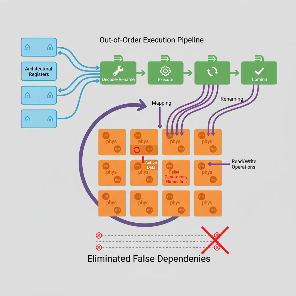
Out-of-Order Execution
Register Renaming
The architectural register file (X0–X30) is far too small to hold the inflight work of a wide OOO core. A physical register file (PRF) of 128–256 entries is allocated dynamically. The rename stage maps each destination register write to a fresh PRF entry, eliminating WAR (Write-After-Read) and WAW (Write-After-Write) hazards while preserving true RAW (Read-After-Write) data dependences.
graph LR
    FETCH["Fetch"] --> DECODE["Decode"]
    DECODE --> RENAME["Register\nRename"]
    RENAME --> DISPATCH["Dispatch"]
    DISPATCH --> ISSUE["Issue"]
    ISSUE --> ALU["ALU\nExecute"]
    ISSUE --> FPU["FP/SIMD\nExecute"]
    ISSUE --> LSU["Load/Store\nUnit"]
    ALU --> WB["Writeback"]
    FPU --> WB
    LSU --> WB
    WB --> COMMIT["Commit\n(Retire)"]

    COMMIT -.->|"Reorder\nBuffer"| DISPATCH
// Visible code — appears serial:
MUL  X1, X2, X3    // WAW: both write X1 ... but after renaming →
ADD  X1, X4, X5    //   MUL  → PRF[p47], ADD → PRF[p48]  (no conflict)

// RAW hazard (cannot rename away):
SDIV X0, X6, X7    // Long latency (≥12 cycles on A78)
ADD  X8, X0, X1    // Must wait for SDIV result in PRF[p47]
Reorder Buffer (ROB)
Instructions are inserted into the ROB in program order at dispatch. They can execute out of order — the ROB records which have completed — but they commit (become visible state) only in program order from the head of the ROB. This is what makes precise exceptions possible: any instruction that faulted can be identified because nothing past it has committed.
Cortex-A55: ~32 entry ROB (in-order up to decode, OOO from issue). Cortex-A78: ~160 entry ROB. Neoverse N2: ~400 entry ROB. Apple Firestorm: ~620 entry ROB — the largest ROB publicly known (2023), enabling deep memory-level parallelism.
Reservation Stations & Execution Ports
// Cortex-A78 issue queues (approximate per ARM TRM):
// IQ0 (integer ALU, shift, CSEL): 4 entries × 2 pipes → 2 ALU/cycle
// IQ1 (multiply, divide):          2 entries × 1 pipe → 1 MUL/cycle
// IQ2 (load):                      12 entries × 2 pipes → 2 loads/cycle
// IQ3 (store):                     8 entries × 1 pipe → 1 store/cycle
// IQ4 (NEON/FP):                   8 entries × 2 pipes → 2 NEON/cycle

// Throughput-limiting example: 4 dependent multiplies, 1 cycle each
MUL  X4, X0, X1    // Uses MUL pipe (1 cycle latency approx)
MUL  X5, X2, X3    // Independent → can dual-issue if separate src regs
MUL  X6, X4, X5    // Depends on X4 and X5 → must wait → serialised
MUL  X7, X6, X3    // Depends on X6 → more serialisation

// Solution: expose more independent chains (see Part 18, multiple accumulators)
Branch Prediction
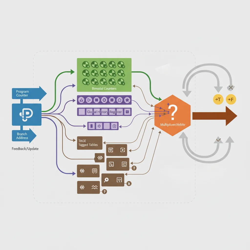
Bimodal & Two-Level Predictors
A bimodal predictor is a table of 2-bit saturating counters indexed by PC bits. Two-level (correlated) predictors index the counter table with a combination of the PC and the Global History Register (GHR), a shift register of the last N branch outcomes. The GHR captures correlation patterns like "this branch is always taken if the last three were also taken."
// Branch that aliases in a bimodal predictor (same PC bits, different ctx):
// Two calls to same function with different condition chains → predictor thrashes
// Solution: pad hot inner loops with NOPs or use PRFM for instruction cache
TAGE Predictor
Tagged GEometric history length (TAGE) uses a base bimodal table plus K tagged tables indexed by hash(PC, GHR[0:2^k−1]). The longest history that hits provides the prediction. A "use-count" meta-predictor arbitrates ties. Cortex-A78 and Neoverse N2 implement variants of TAGE achieving >98% accuracy on SPECint workloads.
How TAGE Works Internally
// ── TAGE Predictor Architecture (simplified) ──
//
//  ┌──────────────┐
//  │  Base Table   │  Bimodal predictor: 2-bit counters indexed by PC
//  │  (T0)         │  Always provides a default prediction
//  └──────┬───────┘
//         │
//  ┌──────┴───────┐  ┌──────────────┐  ┌──────────────┐  ┌──────────────┐
//  │ Tagged T1     │  │ Tagged T2     │  │ Tagged T3     │  │ Tagged T4     │
//  │ History: 4    │  │ History: 16   │  │ History: 64   │  │ History: 256  │
//  │ hash(PC,GHR4) │  │ hash(PC,GHR16)│  │ hash(PC,GHR64)│  │ hash(PC,GHR256)│
//  └──────────────┘  └──────────────┘  └──────────────┘  └──────────────┘
//
// Prediction rule:
//   1. All tables are looked up in parallel using PC+GHR of different lengths
//   2. Each tagged table entry has: { tag, 3-bit counter, 2-bit useful counter }
//   3. The table with the LONGEST matching history provides the prediction
//   4. If no tagged table hits → fall back to base bimodal table T0
//
// Why "GEometric"?
//   Table history lengths grow geometrically: 4, 16, 64, 256, ...
//   This covers patterns at every scale without excessive hardware cost
TAGE on ARM Cores: Parameters by Generation
ARM doesn't publish exact TAGE table sizes (they're proprietary), but TRM documents and academic reverse-engineering reveal approximate parameters:
| Parameter | Cortex-A78 | Neoverse N1 | Neoverse N2 |
|---|---|---|---|
| Predictor Type | TAGE variant | TAGE variant (A76-derived) | Enhanced TAGE |
| Tagged Tables | ~4–5 tables | ~4–5 tables | ~5–6 tables |
| Max History Length | ~200 branches | ~200 branches | ~400+ branches |
| Total Entries (approx) | ~10K | ~10K | ~16K+ |
| SPECint Accuracy | >97% | >97% | >98% |
| Misprediction Penalty | ~11 cycles | ~10 cycles | ~13 cycles (deeper pipeline) |
| Loop Predictor | Yes | Yes | Yes (enhanced) |
| Indirect Predictor | Separate ITT | Separate ITT | Larger ITT + BTAC |
// ── Diagnosing branch predictor behaviour on ARM server cores ──
// PMU event 0x10: BR_MIS_PRED  (mispredicted branches)
// PMU event 0x12: BR_PRED      (correctly predicted branches)
// PMU event 0x21: BR_MIS_PRED_RETIRED (architecturally mispredicted)

// Quick misprediction rate formula:
//   miss_rate = BR_MIS_PRED / (BR_MIS_PRED + BR_PRED)
//
// On Neoverse N2 running SPEC CPU 2017:
//   Typical miss rate: 1.5–2.5% (integer), 0.5–1.5% (floating-point)
//   Compare: Cortex-A55 (no TAGE): 5–10% miss rate on same workloads
//   Compare: Intel Golden Cove (TAGE-like): 1–2% miss rate

// Example: perf on ARM Linux server (Graviton3 / Azure Cobalt):
// $ perf stat -e branches,branch-misses ./my_workload
// Result: 2,000,000,000 branches, 30,000,000 misses → 1.5% miss rate
Branch Target Buffer (BTB) & Return Address Stack (RAS)
While the TAGE predictor decides whether a branch is taken, the Branch Target Buffer (BTB) predicts where it goes — the target address. For conditional branches the target is encoded in the instruction, but for indirect branches (BR Xn, BLR Xn), the BTB must remember previously seen target addresses. The Return Address Stack (RAS) is a specialised predictor for function returns: every BL pushes the return address, and every RET pops it.
// BTB Miss: indirect branch (BR Xn) where target changes frequently
// Triggering BTB miss costs ~20 cycles pipeline flush on A78, ~24 cycles on N2
// Perf event: 0x010 = BR_MIS_PRED
mrs x0, pmcr_el0
// ... configure PMU event 0x010 as in Part 18 ...

// Indirect call via function pointer (high BTB miss rate if target varies):
BLR X9        // BTB must predict X9 content — if wrong: flush + refetch

// Static indirect branches (e.g. switch jump table): BTB usually correct after warmup
// Dynamic virtual dispatch: 1 call site → many targets → BTB capacity exhausted
Return Address Stack (RAS) Depth
The RAS is a small hardware stack that predicts return addresses with near-perfect accuracy for normal call/return patterns. Each BL (Branch-with-Link) pushes the return address onto the RAS; each RET pops the top entry to predict the return target. As long as the call depth doesn't exceed the RAS size, and code doesn't use longjmp, setjmp, or exception-based control flow, the RAS achieves ~99.9% prediction accuracy.
// ── RAS (Return Address Stack) Operation ──
//
// Normal call/return sequence:
BL  func_a      // Push PC+4 onto RAS → RAS: [ret_a]
  BL  func_b    //   Push PC+4 → RAS: [ret_b, ret_a]
    BL  func_c  //     Push PC+4 → RAS: [ret_c, ret_b, ret_a]
    RET         //     Pop ret_c → correct ✓
  RET           //   Pop ret_b → correct ✓
RET             // Pop ret_a → correct ✓

// What breaks the RAS:
// 1. Call depth exceeds RAS size → oldest entries lost
// 2. longjmp/setjmp → unwinding pops don't match pushes
// 3. Exceptions/signals → async stack unwinding corrupts RAS state
// 4. Tail calls (B instead of BL+RET) → RAS not pushed, but no RET to mismatch

// RET vs BR X30:
RET             // Uses RAS predictor → near-instant prediction (0–1 cycle)
BR  X30         // Uses BTB → may miss if X30 value not in BTB → 10–20 cycle penalty
// ALWAYS use RET for function returns, never BR X30| Parameter | Cortex-A55 | Cortex-A78 | Neoverse N1 | Neoverse N2 |
|---|---|---|---|---|
| BTB Entries | ~512 | ~8K | ~8K | ~12K |
| BTB Ways | 2-way | 4-way | 4-way | 4–8 way |
| RAS Depth (entries) | ~8 | ~16 | ~16 | ~32 |
| Indirect Target Table | None | Separate ITT | Separate ITT | Expanded ITT |
| BTB Miss Penalty | ~8 cycles | ~20 cycles | ~18 cycles | ~24 cycles |
BR_MIS_PRED spikes concentrated at function returns, RAS overflow is the likely cause — consider reducing call depth via inlining or restructuring deep call chains.
Memory Subsystem
Store-to-Load Forwarding
A store writes to the store buffer (not directly to cache). A subsequent load to the same address is fulfilled from the store buffer — this is store-to-load forwarding. It avoids the cache latency when the data is still "in flight." However, partial overlaps (e.g., write 8 bytes, read 4 bytes misaligned) cause a forwarding bubble of ~4–8 extra cycles.
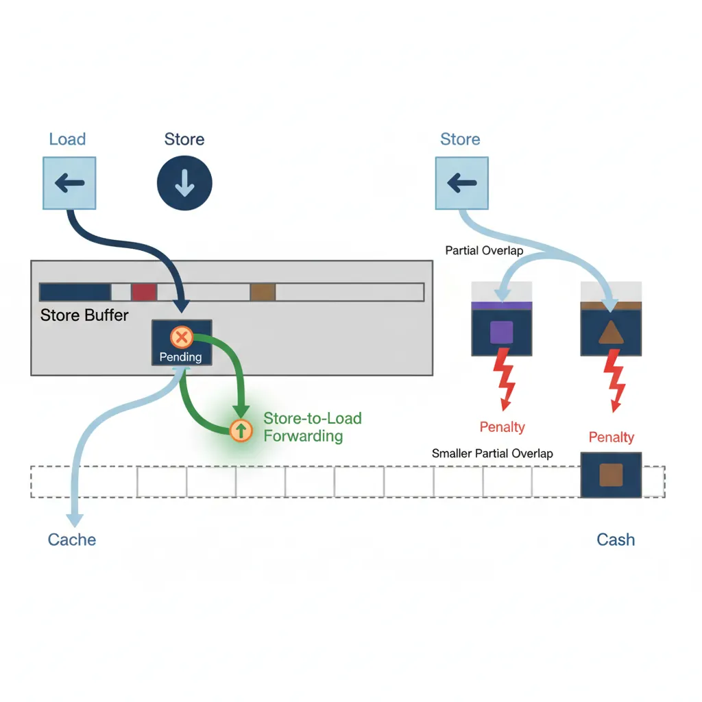
// Perfect forwarding: same address, same size → data from store buffer
STR  X0, [X1]      // Write X0 to [X1]
LDR  X2, [X1]      // Forwarded from store buffer: ~4 cycle latency vs ~12 cache hit

// Forwarding failure: partial overlap
STR  W0, [X1]      // Write 4 bytes to [X1]
LDR  X2, [X1]      // Read 8 bytes from [X1] — only 4 overlap → forwarding stall

// Common kernel bug: write byte, read word (struct alignment pitfall)
STRB W0, [X1]      // 1-byte store
LDR  W2,  [X1]     // 4-byte load → partial overlap → ~10 cycle penalty on A78
Memory Dependence Speculation
ARM OOO cores speculate that loads do not alias most stores. If a load is issued early and a later-dispatched store has the same address, the core detects the violation at commit time, flushes the load (and everything dispatched after it), and re-executes. The PMU event 0x074 = MEM_ACCESS_LD and the perf stat metric memory_bound reveal when this is expensive.
Cache & TLB Architecture
// Query cache parameters at runtime (ARM CTR_EL0):
// CTR_EL0[19:16] = L1 instruction cache line size (log2 words)
// CTR_EL0[3:0]   = L1 data cache line size (log2 words)
mrs  x0, ctr_el0
ubfx x1, x0, #16, #4   // Extract ICache line size field
mov  x2, #4
lsl  x3, x2, x1         // Cache line = 4 << field (bytes)
// On A78: CTR_EL0 = 0x84448004 → L1D line = 64 bytes, L1I line = 64 bytesL1I: 64 KB, 4-way set-assoc, 64-byte lines, 4-cycle hit
L1D: 32 KB, 4-way set-assoc, 64-byte lines, 4-cycle hit
L2 (per core): 256 KB–512 KB, 8-way, 12-cycle hit
L3 (shared): 4–8 MB, 16-way, 30–40 cycle hit
DRAM: 200–300 cycles (DDR5 at 5600 MT/s)
Prefetchers
// Hardware prefetcher types (all implicit, cannot be disabled via ISA):
// 1. Next-line: always fetch the next cache line after a miss
// 2. Stride: detect constant-stride access patterns
// 3. Stream: detect sequential streams, issue ahead-of-time prefetch

// Software prefetch (explicit, from Part 18):
PRFM PLDL1KEEP, [X0, #256]   // Prefetch 4 cache lines ahead into L1D
PRFM PLDL2KEEP, [X0, #512]   // Prefetch into L2 (for long loops)

// PRFM hint types:
// PLDL1KEEP  = load, L1, keep (non-evict hint)
// PSTL1KEEP  = store, L1, keep — prefetch for write (allocate clean line)
// PLDL3STRM  = load, L3, stream (evict-soon hint — scratchpad pattern)
TLB Structure & Shootdown
// TLB Miss: triggers full page table walk (50–200 cycles!)
// TLBI (TLB Invalidate) instructions:
TLBI  VMALLE1IS      // Invalidate all EL1 translations (inner-shareable)
TLBI  VAE1IS, X0     // Invalidate EL1 by virtual address (X0 >> 12 = VA/4KB)
TLBI  ASIDE1IS, X0   // Invalidate all entries with ASID in X0[63:48]
DSB   ISH            // Ensure TLB invalidation visible to all observers
ISB                  // Flush pipeline after TLB change

// TLB shootdown on SMP: each core running threads of the same process
// must invalidate TLBs when a mapping changes. IS (Inner-Shareable) suffix
// broadcasts the TLBI to all cores in the same inner-shareable domain.
Core Comparison
Cortex-A55 (efficiency core used in DynamIQ clusters): In-order up to dispatch; 2-wide decode; 8-entry issue queue; 32-entry ROB equivalent; ~1.9 IPC at peak; sub-1W active power. Designed for background tasks and always-on workloads.
Cortex-A78 (performance core, 2020–2023 smartphones): 4-wide decode; 160-entry ROB; 6 execution ports; 2 load + 1 store / cycle; TAGE branch predictor; 3.6 IPC peak; ~2.5W TDP in 5 nm silicon.
Neoverse N2 (server, 2022+): 4-wide decode; 400-entry ROB; 8 execution ports; 3 load + 2 store / cycle (SVE adds vector load/store ports); CHI interconnect for cache coherence at rack scale; ~4.0 IPC peak; 10W+ TDP.
Neoverse N1 — ARM's Datacenter Breakthrough
Neoverse N1 is ARM's first-generation server-class core. It is derived from the same Cortex-A76 "Enyo" microarchitecture that revolutionized mobile performance in 2018, but re-tuned for throughput, reliability, and multi-socket server environments. Think of it as the A76's older sibling who traded the thin smartphone chassis for a well-cooled server rack.
N1 Microarchitecture at a Glance
// ── Neoverse N1 Front-End ──
// Fetch:  4-wide fetch, up to 8 instructions per cycle from op cache
// Decode: 4-wide decode (same as A76) — fixed-length ISA simplifies this
// Op Cache: ~1,500 µop cache (inherited from A76, bypasses decode)
// Branch Predictor: TAGE variant, >97% accuracy on server workloads

// ── N1 Back-End (Out-of-Order Engine) ──
// ROB:   ~128 entries (same depth as A76 — prioritizing per-core efficiency)
// Issue:  8 issue slots → 6 execution ports
// Ports:  2× integer ALU, 1× multiply/divide, 2× load, 1× store
// SIMD:   2× 128-bit NEON pipes (no SVE on N1 — SVE arrived with N2)

// ── N1 Memory Subsystem (server-optimised) ──
// L1I: 64 KB, 4-way
// L1D: 64 KB, 4-way  (double the typical mobile A76 L1D of 32 KB)
// L2:  512 KB–1 MB per core (configurable by SoC vendor)
// L3:  Shared via CMN-600 mesh — up to 32 MB per chip
// Coherence: AMBA CHI (Cache-Coherent Hub Interface) for multi-chip systems
What N1 Changed vs Mobile A76
Although N1 shares A76's core pipeline, ARM made targeted modifications for server workloads:
| Feature | Cortex-A76 (Mobile) | Neoverse N1 (Server) | Why It Changed |
|---|---|---|---|
| L1D Cache | 32 KB | 64 KB | Server workloads have larger working sets |
| L2 Cache | 256–512 KB | 512 KB–1 MB | Database/web server hot data is larger |
| Interconnect | DSU (4-core cluster) | CMN-600 mesh (up to 128 cores) | Scale to server-grade core counts |
| RAS (Reliability) | Basic | Full ARMv8.2 RAS | ECC, error injection, fault recovery for 24/7 uptime |
| Virtualisation | ARMv8.2 | ARMv8.2 + nested virt hints | Cloud providers run thousands of VMs per host |
| Crypto | AES/SHA | AES/SHA + SM3/SM4 | Chinese crypto standards for global cloud markets |
| Power Target | ~1.5W per core (5 nm) | ~1W per core (7 nm, efficiency-optimised) | 128-core chip must fit in a 200W TDP envelope |
N1 in the Real World: AWS Graviton2
How Graviton2 Changed Cloud Computing
AWS designed the Graviton2 processor around 64 Neoverse N1 cores on a single chip, manufactured at TSMC 7nm. When it launched in 2020, it became the most successful ARM server deployment in history:
- 64 cores / 64 threads — no SMT (each core is a full pipeline, simplifying scheduling)
- 32 MB shared L3 via CMN-600 mesh interconnect
- 8-channel DDR4-3200 — 307 GB/s memory bandwidth
- ~40% better price-performance vs Intel Xeon (m6g vs m5 instances)
- ~20% lower power — N1's efficiency means AWS could pack more compute per rack
Key insight: Graviton2 didn't try to win on single-thread speed (N1's 128-entry ROB is modest). Instead, it won on throughput per watt per dollar — packing 64 efficient cores where Intel offered 32 power-hungry ones. This is the same design philosophy that made ARM dominant in mobile, now applied to the datacenter.
Impact: After Graviton2's success, every major cloud provider followed — Microsoft built Azure Cobalt (Neoverse N2), Google deployed Axion (N2-based), and Oracle adopted Ampere Altra (N1-based). ARM server market share grew from <1% (2019) to ~15% (2024).
N1 → N2 → N3: The Neoverse Roadmap
Understanding where N1 sits in ARM's server roadmap helps contextualise performance expectations:
| Core | Year | Base | Decode | ROB | SVE | Key Cloud Chip |
|---|---|---|---|---|---|---|
| Neoverse N1 | 2019 | A76 | 4-wide | ~128 | None | AWS Graviton2, Ampere Altra |
| Neoverse V1 | 2020 | X1 | 5-wide | ~288 | SVE 256-bit | AWS Graviton3 |
| Neoverse N2 | 2022 | A710 | 5-wide | ~400 | SVE2 128-bit | Azure Cobalt 100, Google Axion |
| Neoverse V2 | 2023 | X3 | 5-wide | ~400+ | SVE2 128-bit | AWS Graviton4, NVIDIA Grace |
| Neoverse N3 | 2025 | A725 | 6-wide | ~450+ | SVE2 | (upcoming deployments) |
PRFM) across NUMA boundaries matters more.
Neoverse N2 — The Cloud-Native Workhorse
Neoverse N2 (2022) is ARM's second-generation cloud-native server core. While N1 was derived from the mobile Cortex-A76, N2 is based on Cortex-A710 — the first ARMv9 mid-core. ARM redesigned the front-end (5-wide decode, larger TAGE, expanded BTB), deepened the out-of-order engine (400-entry ROB, more execution ports), and added SVE2 for vector workloads. N2 powers Microsoft Azure Cobalt 100 (128 cores), Google Axion, and Ampere AmpereOne.
N2 Microarchitecture — Full Breakdown
// ── Neoverse N2 Front-End ──
// Fetch:  8-wide fetch (2× the visible 5-wide decode width)
// Decode: 5-wide decode (vs 4-wide on N1) — 25% more instructions per cycle
// Op Cache: ~3,000 µop cache (doubled vs N1's ~1,500)
// Branch Predictor: Enhanced TAGE, ~5–6 tagged tables
//   - Max history depth: ~400 branches (vs ~200 on N1)
//   - SPECint accuracy: >98%
//   - Separate loop predictor for counted loops
// BTB: ~12K entries, 4–8 way (vs ~8K on N1)
// RAS: ~32 entries deep (vs ~16 on N1)
// Misprediction penalty: ~13 cycles (deeper pipeline than N1's ~10)

// ── N2 Back-End (Out-of-Order Engine) ──
// ROB:   ~400 entries (3× deeper than N1's ~128)
// Issue:  10 issue slots → 8 execution ports
// Ports:  2× integer ALU + 1× integer ALU/branch
//         1× multiply/divide
//         3× load (vs 2 on N1)
//         2× store (vs 1 on N1)
//         2× 128-bit NEON/SVE2 pipes
// SVE2:  128-bit vector length (fixed, not scalable on N2)
//        Enables: bit manipulation, crypto, ML inference instructions

// ── N2 Memory Subsystem ──
// L1I: 64 KB, 4-way set-associative, 64-byte lines
// L1D: 64 KB, 4-way set-associative, 64-byte lines
// L2:  1 MB per core (fixed, not configurable like N1)
// L3:  Shared via CMN-700 mesh — up to 64 MB per chip
//      (CMN-700 replaces N1's CMN-600 — lower latency, more cross-links)
// Coherence: AMBA CHI, CXL-ready for memory expansion
// DRAM: DDR5-5600 support via SoC integration
N2 Cache Architecture — The 64 KB 4-Way Design
Both N2's L1 instruction cache and L1 data cache are 64 KB, 4-way set-associative with 64-byte cache lines. This is a deliberate balance between hit rate and access latency:
Capacity (64 KB): Server workloads (web servers, databases, JIT compilers) have larger hot instruction footprints than mobile apps. A 32 KB L1I would thrash on a typical PostgreSQL query executor path. 64 KB captures most hot code paths without increasing access latency beyond ~4 cycles.
Associativity (4-way): With 64-byte lines and 64 KB capacity, each way holds 256 sets. 4-way associativity means 4 different cache lines can map to the same set index before eviction — this significantly reduces conflict misses compared to 2-way (which the A55 uses). Going to 8-way would increase hit rate marginally but add ~1 cycle access latency — not worth it for L1.
64-byte lines: Match the AMBA CHI bus transfer granularity and align with DRAM burst lengths. Prefetching operates at cache-line granularity, so every L1 miss fetches exactly 64 bytes from L2.
| Cache Level | Neoverse N1 | Neoverse N2 | Impact of Change |
|---|---|---|---|
| L1I | 64 KB, 4-way | 64 KB, 4-way | Same — proven size for server instruction locality |
| L1D | 64 KB, 4-way | 64 KB, 4-way | Same — optimal for server data working sets |
| L1 Hit Latency | ~4 cycles | ~4 cycles | Critical path unchanged |
| L2 (per core) | 512 KB–1 MB | 1 MB (fixed) | Consistent sizing simplifies SoC integration |
| L2 Hit Latency | ~10 cycles | ~12 cycles | Slightly deeper due to wider data paths |
| L3 (shared) | Up to 32 MB (CMN-600) | Up to 64 MB (CMN-700) | 2× capacity for larger workload isolation |
| L3 Hit Latency | ~30–40 cycles | ~35–45 cycles | Mesh topology adds 5 cycles but reduces contention |
N1 vs N2: What Changed and Why
Generational Leap: N1 → N2
The jump from N1 to N2 is one of the largest generational improvements in ARM server history. Here's why each change mattered:
| Feature | Neoverse N1 | Neoverse N2 | Why It Matters |
|---|---|---|---|
| ISA | ARMv8.2 | ARMv9.0 | MTE, BTI, PAUTH2 — hardware security baseline |
| Decode Width | 4-wide | 5-wide | 25% more decode throughput per cycle |
| ROB Depth | ~128 | ~400 | 3× deeper OOO window → far more memory-level parallelism |
| Execution Ports | 6 | 8 | More parallel execution units |
| Load Ports | 2 | 3 | 50% more memory bandwidth per core |
| Store Ports | 1 | 2 | 2× store throughput — critical for memcpy, database writes |
| TAGE History | ~200 branches | ~400+ branches | Better prediction for deep server call stacks |
| BTB Size | ~8K | ~12K | More indirect branch targets cached |
| RAS Depth | ~16 | ~32 | No overflow on typical 20–30 deep server call stacks |
| SVE Support | None | SVE2 (128-bit) | Crypto, ML inference, bitmanip acceleration |
| Interconnect | CMN-600 | CMN-700 | Lower latency mesh, CXL-ready |
| Perf vs N1 | Baseline | ~40% single-thread IPC | Largest generational IPC gain in Neoverse history |
Design philosophy: N1 was a "prove it can work" core — conservative ROB, no SVE, mobile DNA. N2 is a purpose-built server core — 400-entry ROB rivals Intel's Golden Cove, 5-wide decode matches AMD Zen 4, and SVE2 provides the vector extensions that HPC and ML inference demand. The result: N2 closes the single-thread IPC gap with x86 to within ~5%, while maintaining ARM's 2–3× better performance-per-watt advantage.
PRFM aggressively and unroll loops deeper to exploit memory-level parallelism; (2) 3 load ports means three independent loads can issue per cycle — interleave load-heavy code with compute; (3) SVE2 is available but fixed at 128-bit on N2 — don't expect wider vectors (use CNTB to query vector length at runtime); (4) misprediction penalty is ~13 cycles (vs ~10 on N1) due to the deeper pipeline — branch-heavy code pays a higher cost per miss.
Assembly Implications
// ── Rule 1: Break dependence chains for ILP ──
// Bad: chain of 4 multiplies → 1 result/4 cycles
MUL  X0, X1, X2
MUL  X0, X0, X3
MUL  X0, X0, X4
MUL  X0, X0, X5

// Good: 4 independent multiplies → 4 results/1 cycle (wide issue)
MUL  X0, X1, X2
MUL  X6, X3, X4
MUL  X7, X5, X8
MUL  X9, X10, X11
// Then merge: MUL X12, X0, X6 / MUL X13, X7, X9 / MUL X0, X12, X13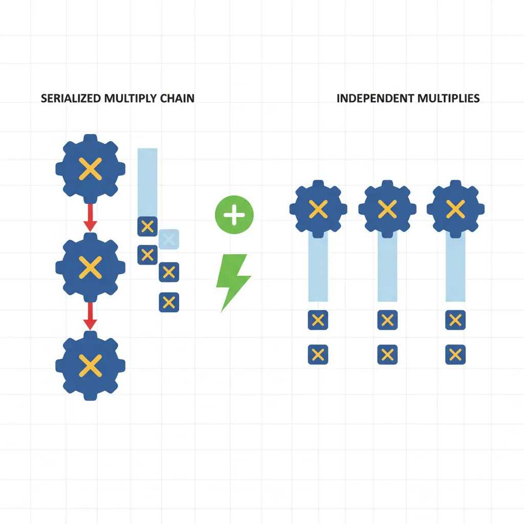
// ── Rule 2: Avoid indirect branch thrash → prefer direct branches ──
// VTable dispatch: BLR Xn — poor BTB predictions when targets vary
// Alternative: inline or devirtualise in hot paths
// ── Rule 3: Align hot loop head to I-Cache line boundary ──
.balign 64 // 64-byte = L1I cache line on A78
.loop_head:
LDP X0, X1, [X2], #16
LDP X3, X4, [X2], #16
// ... loop body ...
B.NE .loop_head// ── Rule 4: Separate store and load to same address ──
STR X0, [X1]
// Insert ~4 independent instructions here to allow forwarding pipeline
ADD X5, X6, X7 // Fill cycle 1
ADD X8, X9, X10 // Fill cycle 2
ADD X11, X12, X13 // Fill cycle 3 (A78 forwarding latency ≈ 4)
LDR X2, [X1] // Now forwarding hits clean without stallCase Study: Apple M1 vs Cortex-X2 — Two Takes on Wide OOO
How Different Design Philosophies Yield Different Results
When Apple's M1 (Firestorm cores) launched in 2020, it shattered ARM performance expectations. Its microarchitecture makes a fascinating comparison to ARM's own Cortex-X2 (2022):
| Parameter | Apple Firestorm (M1) | Cortex-X2 |
|---|---|---|
| Decode Width | 8-wide | 5-wide |
| ROB Size | ~630 entries | ~288 entries |
| Integer ALU Ports | 6 | 4 |
| Load/Store Ports | 3 Load + 2 Store | 2 Load + 2 Store |
| L1D Cache | 128 KB, 8-way | 64 KB, 4-way |
| L2 Cache (per core) | 12 MB shared (perf cluster) | 512 KB–1 MB |
| Power Target | ~10W (perf cluster) | ~3W (single core) |
Key insight: Apple's advantage comes from being both the chip designer and the only customer — they can afford a 630-entry ROB and 128 KB L1D because they control the thermal design of the MacBook chassis. ARM's Cortex-X2 must work across dozens of Android phones with different thermal budgets, forcing a more conservative design. The lesson: microarchitecture trade-offs are inseparable from the system they ship in.
Performance impact: On SPEC CPU 2017, Firestorm's wider issue and larger ROB deliver ~15–20% higher single-thread IPC than X2, but X2's smaller area allows more cores per cluster. In server workloads (Neoverse N2), throughput per watt matters more than single-thread speed, so ARM chose a 4-wide balanced design instead.
From StrongARM to Neoverse: 30 Years of ARM Microarchitecture
ARM microarchitecture has evolved through distinct generations:
- 1996 — StrongARM (DEC, then Intel): The first high-performance ARM core. 5-stage in-order pipeline, 233 MHz, 1W. Proved ARM could compete on performance, not just power.
- 2005 — Cortex-A8: ARM's first superscalar core. 2-wide in-order, dual-issue integer. Powered the original iPhone (2007) and Kindle.
- 2011 — Cortex-A15: ARM's first fully out-of-order core. 3-wide decode, ~100-entry ROB. The architecture that made ARM credible for servers (Calxeda, Applied Micro).
- 2018 — Cortex-A76 ("Enyo"): 4-wide OOO, 128-entry ROB, micro-op cache. Closed the gap with Intel mobile Core i5. Basis for Neoverse N1 (AWS Graviton2).
- 2022 — Neoverse V2: 5-wide decode, SVE2, 400+ ROB, CHI mesh interconnect. Powers Graviton4 and Microsoft Cobalt — ARM's entry into datacenter dominance.
Each generation roughly doubled ROB size and added 1–2 execution ports, a pattern constrained by the cubic relationship between power and OOO window size.
Hands-On Exercises
Measure ROB Depth via Dependency Chain
Empirically estimate your CPU's ROB size by measuring when independent instruction throughput drops:
- Write a loop containing N independent
ADD Xn, Xn, #1instructions (each writing a different register), followed by a single long-latencySDIVwhose result is consumed by the next iteration's first ADD - Increase N from 10 to 300 in steps of 10. Time 10 million iterations of each
- Plot cycles/iteration vs N. While N < ROB depth, the independent ADDs fill the ROB and overlap with the SDIV. Once N exceeds the ROB, dispatching stalls — the curve flattens
- The "knee" of the curve approximates the ROB size
Expected: On Cortex-A78, the knee should appear around N=150–160. On Apple M-series, around N=600+.
Branch Predictor Stress Test
Design a benchmark that defeats TAGE prediction:
- Create an array of 256 random 0/1 values (unseeded random — different each run)
- Loop through the array; for each element, execute
CBZ/CBNZto branch into one of two code paths - Measure total cycles and branch mispredictions using PMU events
0x10 (BR_MIS_PRED)and0x12 (BR_PRED) - Compare against a sorted version of the same array (all 0s then all 1s) — mispredictions should drop to near-zero
Analysis: Calculate misprediction rate for random vs sorted. Typical results: ~45-50% miss rate on random (worse than coin flip due to aliasing), <1% on sorted.
Store-to-Load Forwarding Latency Measurement
Measure the difference between forwarded and non-forwarded loads:
- Write a tight loop:
STR X0, [X1] / LDR X2, [X1](same address, same size — perfect forwarding). Time 100M iterations using cycle counter - Modify to misaligned partial overlap:
STR X0, [X1] / LDR W2, [X1, #2](4-byte load at 2-byte offset into 8-byte store). Time again - Modify to complete miss:
STR X0, [X1] / LDR X2, [X3]where X3 points to a different cache line - Calculate: forwarding latency, partial-overlap penalty, and L1D hit latency (from the miss case)
Expected on A78: ~4 cycles (forwarded), ~10-12 cycles (partial overlap), ~4 cycles (L1D hit, no forwarding — same if data is warm in cache).
Conclusion & Next Steps
The Cortex-A78 represents the intersection of every concept in the series: ISA constraints shape what rename can do, weak memory ordering emerges from the store buffer design, and cache line boundaries determine when PRFM helps. Every assembly optimization from Part 18 maps to a physical circuit now visible in this part. The Apple M1 vs Cortex-X2 comparison shows how system-level constraints drive wildly different microarchitectural choices from the same ISA, and the exercises let you probe these mechanisms empirically by measuring ROB depth, branch predictor accuracy, and forwarding latency on real hardware.